Advanced Search

Current Issue

2025 Vol. 47, No. 9

2025, 47(9)
Abstract:
2025, 47(9): 1-4.
Abstract:
Excellence Action Plan Leading Column
Space-based Computing Chips: Current Status, Trends and Key Technique
WEI Xiaotong, XU Haobo, YIN Chundi, HUANG Junpei, SUN Wenhao, XU Wenjun, WANG Ying, LIU Yaoqi, MENG Fantao, MIN Feng, WANG Mengdi, HAN Yinhe
2025, 47(9): 2963-2978. doi: 10.11999/JEIT250633
Abstract:
  Significance   With the continuous advancement of aerospace technology and the growing demand for space applications, space-based computing chips have assumed increasingly important strategic roles as core hardware infrastructure of space information systems. As the technological foundation enabling intelligent data processing and reliable communications for spacecraft—including satellite platforms, space stations, and deep space probes, space-based computing chips not only safeguard national security and support economic development but also play an irreplaceable role in serving civilian needs. Although existing survey literature has systematically reviewed the development of aerospace Central Processing Units (CPUs), comprehensive analyses of other key components within the space-based computing chip ecosystem remain limited. To address this gap, this paper systematically examines the technological evolution of various space-based computing chips and their principal fault-tolerant mechanisms, and further explores potential future trends in this field.  Progress   This paper adopts a functional architecture-oriented classification to systematically analyze and summarize the current technological status of space-based computing chips across three dimensions: CPU, Field-Programmable Gate Array (FPGA), and dedicated chip. For CPU technology, a classification study of general-purpose processors widely used in aerospace applications is conducted based on instruction set architectures, with in-depth analysis of the technical characteristics and representative products of various architectures, together with an objective evaluation of their advantages and limitations in space environments. In the FPGA domain, the technical specifications and performance characteristics of mainstream space-grade FPGA products, both domestic and international, are comprehensively reviewed to provide a reference for application selection. For dedicated chips, a detailed categorization is carried out according to functional architectural features and application scenario requirements, covering Digital Signal Processing (DSP) chips for signal processing acceleration, Graphics Processing Unit (GPU) chips for graphics computation, and Neural Processing Unit (NPU) chips for space-based artificial intelligence applications, thereby systematically clarifying the applicability of different architectures in complex space environments. In addition, this paper presents an in-depth analysis of the key fault-tolerant technology framework for space-based computing chips at multiple levels, including system, architecture, circuit, and process library, and provides a comprehensive evaluation of the technical advantages, application limitations, and development prospects of various fault-tolerant mechanisms. This analysis offers theoretical guidance for the reliability design of space-based computing chips.  Conclusions  This review systematically summarizes the technological development of space-based computing chips, providing a comprehensive analysis of the architectural characteristics of different chip types and their associated fault-tolerant technology frameworks, while elucidating the applicable scenarios and technical limitations of various fault-tolerant mechanisms. The central principle of fault-tolerant design for space-based computing chips is to achieve effective detection and correction of circuit faults through redundancy mechanisms. This paper offers an in-depth analysis of the implementation principles and application characteristics of fault-tolerant technologies at four hierarchical levels: system, architecture, circuit, and process library. Although these multi-level approaches substantially improve system reliability, they inevitably introduce hardware resource overhead and performance penalties. Therefore, the engineering design of space-based computing chips requires optimized strategies that combine multi-level fault-tolerant technologies according to specific reliability requirements, aiming to balance reliability, cost, and performance to meet the intended design objectives and technical specifications.  Prospects   Looking ahead, space-based computing chips present broad prospects in high computing capability, widespread adoption of Commercial Off-The-Shelf (COTS) devices, and the development of Reduced Instruction Set Computer-Five (RISC-V) instruction set architectures. With the rapid advancement of space technology, space-based systems are undergoing a transformation from traditional single-function platforms to integrated platforms characterized by multi-task collaboration, autonomy, and intelligence. Real-time data processing, multi-task parallel computing, and intelligent decision-making have become the principal driving forces in the evolution of space-based computing technology, all of which demand robust computational foundations. Compared with traditional radiation-hardened specialized devices, COTS devices are emerging as a major trend in space-based computing chip development due to their advantages in cost-effectiveness, computational performance, shorter development cycles, and product diversity. In addition, RISC-V, as an open-source instruction set architecture, offers unique advantages and significant potential for space-based computing chip innovation through its modular design philosophy, exceptional scalability, and open ecosystem. Chiplet technology, as an innovative approach to chip design and fabrication, enables cost reduction and accelerates development timelines through its modular architecture, while simultaneously facilitating flexible customization and fault-tolerant mechanisms. This approach is particularly well-positioned to address the evolving and heterogeneous computing demands of space-based platforms.
A 64 Gb/s Single-Ended Simultaneous Bi-Directional Transceiver for Die-to-Die Interfaces
WANG Zhifei, HUANG Zhiwen, YE Tianchen, YE Bingyi, LI Fangzhu, WANG Wei, YU Dunshan, GAI Weixin
2025, 47(9): 2979-2993. doi: 10.11999/JEIT250506
Abstract:
  Objective  Chiplet technology, which packages multiple dies with different functions and processes together, offers a cost-effective way for fabricating high-performance chips. For die-to-die data transmission, the edge density, Bit Error Rate (BER), and power consumption of the interface are crucial to the chip’s key performance metrics, such as computing power and throughput. Simultaneous Bi-Directional (SBD) signaling is an effective way to double the edge density by transmitting and receiving data on the same channel. However, with higher data rate and smaller channel pitch, channel reflection and crosstalk bring severe challenges to the design of interface circuits. This paper presents a single-ended SBD transceiver with echo and crosstalk cancellation to achieve a larger edge density and a lower BER.  Methods  The transceiver improves the per-wire data rate by utilizing the SBD signaling and denser shield-less channels. However, as both ends of the channel transmit data simultaneously, bi-directional signal coupling arises. Signal coupling, echo from impedance mismatch, and crosstalk from adjacent channels degrade the received data’s Signal-to-Noise Ratio (SNR). To decouple the bi-directional signal and cancel the echo and Near-End Crosstalk (NEXT), this paper proposes a Dynamic Voltage ThresHold generator (D-VTH). It generates the slicer’s threshold voltage according to the interfering signals needing to be subtracted. To cancel the Far-End Crosstalk (FEXT), a channel with the same capacitive and inductive coupling is designed by adjusting its width and space. FEXT is the subtraction of these two kinds of coupling, so it is canceled as expected. The source-synchronize architecture enhances the clock-data tracking performance, thereby reducing the clock-to-data jitter to improve the link’s noise margin. The synchronous clock distribution circuit includes a standing wave-based half-rate clock (CK2) distribution and a delay-controlled reset chain. The end of the CK2’s Transmission Line (TL) is terminated by a dedicated inductor, making the reflected wave have a proper amplitude and phase relative to the incident wave; thus, a standing wave can be formed, and CK2 synchronization is realized. To ensure the divided clocks (up to 1/32-rate) are synchronous, the dividers’ reset signals must be released at the same time or skewed with an integer multiple of 32 Unit Interval (UI). A reset chain is proposed to release the reset signals with controlled delay. The delay increases by 2 UI at each lane and is compensated by different stages of DFFs. After the CK2 and the divided clocks’ synchronization, the transmitter’s output and NEXT cancellation synchronization are achieved.  Results and Discussions  The test chip, including the proposed transceiver and the 3 mm on-chip channel, is fabricated in 28 nm CMOS. The shield-less data channels are routed in the M9 layer, with a channel pitch of 6.1 um. An electromagnetic field solver calculates the channel’s frequency response and the equivalent lumped model. The equivalent \begin{document}$ {C}_{\mathrm{m}}/{C}_{\mathrm{s}} $\end{document} is 0.28, and the \begin{document}$ {L}_{\mathrm{m}}/{L}_{\mathrm{s}} $\end{document} is 0.26, making FEXT 24 dB smaller than the Insertion Loss (IL) at the Nyquist frequency. In contrast, NEXT and Return Loss (RL) are much larger; they are just 7.3 dB and 8.3 dB smaller than the IL at the Nyquist frequency, respectively (Fig.12). The D-VTH filter’s coefficients are obtained from the Sign-Sign Least Mean Square (SS-LMS) adaptation algorithm, and the data is received correctly using the adapted coefficients. The bi-directional decoupling coefficient is the largest because the local transmitter’s output is the strongest compared to the echo and crosstalk. The echo cancellation coefficient is the smallest because it has to undergo additional insertion loss in the channel (Fig.13). The simulated clock-to-data tracking performance shows the transceiver’s robustness against power supply noise (Fig.15). The standing wave distribution’s simulation results show its amplitude is double that of the conventional traveling wave because of the superposition of incident and reflected waves. A slight skew of 0.6 ps is observed, caused by the residual traveling wave due to the TL’s loss (Fig.18). The measured internal eye diagrams and bathtub curves at 64 Gb/s shows the eye-opening is 0.68 UI/80 mV at 10–9 BER and 0.64 UI/77 mV at 10–12 BER, with both crosstalk cancellation and echo cancellation enabled (Fig.21). In addition, the measured BER at the optimal sampling point is less than 10–16 with all the lanes counting bit errors. The Crosstalk-Induced Jitter (CIJ) is reduced from 0.58 UI to 0.06 UI after crosstalk cancellation is enabled, representing a reduction ratio of 89.6% (Table 1). The measured power efficiency is 1.21 pJ/b, and the simulated power breakdown shows that the transmitter, receiver, D-VTH, and clock distribution account for 40%, 23%, 34%, and 3%, respectively (Fig.22). This work achieves the best per-wire data rate and per-layer edge density compared with previous works (Table 2).  Conclusions  This paper utilizes SBD signaling and denser shield-less channels to achieve a per-wire data rate of 64 Gb/s and a per-layer edge density of 10.5 Tb/(s·mm). The proposed echo and crosstalk cancellation circuit ensures an extremely low BER of less than 10–16. It provides new insights for increasing the edge density of die-to-die interfaces.
Co-design of Architecture and Packaging in Chiplet
LU Meixuan, XU Haobo, WANG Ying, WANG Mengdi, HAN Yinhe
2025, 47(9): 2994-3009. doi: 10.11999/JEIT250626
Abstract:
  Significance   Chiplet technology, enabled by advanced packaging techniques, integrates multiple chiplets into a single package to form a larger-scale chip system. This approach breaks through the “Area Wall” faced by traditional processes and has become a critical path for improving computing performance in the post-Moore era. The design flexibility afforded by packaging-level integration has created a new design paradigm that drives iterative advances in computing and integration architectures. In traditional monolithic chip design, architecture and packaging are relatively independent stages. By contrast, the ability to integrate chiplets fabricated in different processes and the scalability of chiplet technology greatly expand the design space but also increase design complexity. At the same time, the higher transistor density per unit volume intensifies multi-physics coupling effects, including thermal, mechanical, and electrical interactions. Therefore, traditional methods that rely solely on packaging design to address performance degradation and reliability issues are no longer sufficient for chiplet-based systems. Instead, architecture and packaging in chiplet design must be co-designed in a coordinated manner.  Progress   This work addresses the critical issues of architecture-packaging co-design in the context of chiplet systems. It reviews architectural design and co-optimization efforts, demonstrates the necessity of co-design, and proposes co-design optimization methodologies. First, it summarizes architectural characteristics and development trends driven by advanced packaging technologies. These technologies are categorized into 2D, 2.5D, 3D, and 3.5D integration according to chiplet arrangement and interconnection technologies, each leading to substantial architectural differences. A detailed comparison of packaging technologies is provided, outlining the architectural features and co-design considerations associated with each. The necessity of co-design is then clarified from the perspective of the profound effect of packaging technologies on performance and reliability. The increased integration density per unit volume in chiplet-based circuits introduces serious reliability challenges, including complex multi-physics coupling effects such as thermal, mechanical, and electrical interactions. Multiple research studies on chiplet reliability are cited, highlighting the severity of thermal, mechanical, and electrical problems arising from these couplings. Unlike traditional monolithic chip designs, reliability issues in chiplet-integrated circuits cannot be resolved through standalone packaging-level design. Separate design of architecture and packaging introduces performance risks and leads to unpredictable design and manufacturing timelines and costs. Therefore, co-design of architecture and packaging is a necessary trend for the advancement of chiplet-based circuits. Finally, by reviewing existing cross-layer co-optimization efforts, an architecture-packaging co-optimization methodology is proposed to provide guidance for design optimization. Key design factors and evaluation metrics at both the architectural and packaging levels are summarized, and the interfaces for cross-layer co-design are clarified. The co-design interface consists of two components: design factors and evaluation metrics. Adjustments to any design factor within the design space affect multiple evaluation metrics, which in turn drive the convergence of the design space. Two key components are summarized for each design layer: (1) the definition of the design parameter space and exploration methods, and (2) the selection of evaluation metrics together with evaluation models and methodologies. The co-design process is outlined in eight key steps, illustrated by prior works. Existing architecture-packaging co-design methods are reviewed, and design workflows are categorized and characterized.  Conclusions  Driven by the evolution of chiplet technology and objectives such as performance and cost, chiplet-integrated circuit architectures have developed characteristics that differentiate them from traditional monolithic designs. The strong coupling between architecture and packaging layers has substantially increased design complexity, while higher integration density has introduced intricate multi-physics interactions, elevating reliability risks. The traditional design paradigm, in which architecture and packaging are developed independently, now faces challenges including performance degradation, unpredictable verification timelines, and uncontrollable costs. Co-design has therefore emerged as a critical solution. Establishing cross-layer collaborative methods and making trade-offs among multidimensional objectives are essential. By defining the design spaces for both architecture and packaging, formulating efficient exploration strategies, and applying system- and packaging-level evaluation methods, it becomes possible to rapidly and accurately identify optimal design solutions. Architecture-packaging co-design enables performance, reliability, and other objectives to be optimized synergistically at the early stages of chiplet-integrated circuit design with minimal cost. This approach maximizes the benefits of high integration density while mitigating risks in chip design and manufacturing.  Prospects   Architecture-packaging co-design represents the future paradigm for chiplet design. Current co-design approaches remain limited in applicability: methods that rely on detailed models such as RTL and netlists, together with EDA tools, are unsuitable for early-stage chip development, whereas abstract modeling techniques may neglect critical design issues and introduce substantial inaccuracies. Future co-design methodologies must adapt to different stages of the design process and support the iterative advancement of both computing architectures and integration architectures.
Overviews
Overview of Stochastic Computing Applications and Challenges
CHEN Lu, WANG Jiangyuan, ZHONG Kuncai, ZHANG Jiliang
2025, 47(9): 3010-3019. doi: 10.11999/JEIT250413
Abstract:
  Significance   This paper systematically organizes and analyzes the historical progress, fundamental characteristics, application scenarios, and challenges of Stochastic Computing (SC), making four main contributions. (1) Integration of theoretical frameworks and refinement of knowledge systems. By reviewing the evolution of SC from its theoretical origins in the 1940s to its resurgence in the 21st-century Internet of Things era, the paper establishes a coherent theoretical trajectory. The analysis of unipolar and bipolar encoding mechanisms, stochastic bitstream generation architectures, and computational error models provides researchers with a unified technical framework. (2) Demonstration of application potential. Through examinations of three representative scenarios, namely digital filters, image processing, and neural networks, the paper highlights SC’s advantages in hardware efficiency and fault tolerance. For instance, XNOR-gate and multiplexer-based digital filter designs reduce hardware resource consumption by several orders of magnitude, whereas neural network acceleration schemes that employ low-discrepancy sequence-based stochastic sources markedly improve energy efficiency in edge AI devices. These case studies provide implementable technical pathways for engineering practice. (3) Identification of critical challenges and evaluation of solutions. Addressing three major challenges, including correlation accumulation, excessive hardware overhead in random number generation, and the precision-efficiency trade-off, the paper not only quantifies their technical origins but also evaluates the effectiveness and limitations of existing solutions, offering clear optimization directions for further research. (4) Strategic guidance for future research. By integrating emerging technological trends, the paper proposes directions such as algorithm-hardware co-design, dynamic correlation suppression, and adaptive precision adjustment. Special emphasis is placed on the potential of reconfigurable methods and novel architectures to overcome current bottlenecks, outlining research frontiers for both academia and industry.  Conclusions   This paper systematically reviews the historical development and foundational principles of SC, elaborates on representative application scenarios, and examines the core technical challenges it currently faces. Compared with traditional deterministic numerical computation, SC offers advantages including low hardware overhead, high asymptotic precision, and strong fault tolerance, which have enabled its adoption in digital signal processing, neural network acceleration, and edge computing. Nevertheless, several critical challenges persist and must be resolved to advance its practical deployment.  Prospects   As a promising pathway to address the computing power and energy efficiency challenges of the post-Moore era, the future development of SC will emphasize overcoming technical bottlenecks and adapting to emerging application scenarios. Advances in reconfigurable computing architectures, memristor-based memory devices, and compute-in-memory chips provide new opportunities for architectural innovation and performance optimization of SC systems. These developments further enhance its intrinsic advantages of low power consumption, high fault tolerance, and progressive precision, positioning SC as a key technological foundation for building high-efficiency computing systems in the post-Moore era.
A Survey of Processor Hardware Vulnerability
LAN Zeru, QIU Pengfei, WANG Chunlu, ZHAO Yaxuan, JIN Yu, ZHANG Zhihao, WANG Dongsheng
2025, 47(9): 3020-3037. doi: 10.11999/JEIT250357
Abstract:
  Significance  Processor security is a cornerstone of computer system security, providing a trusted execution environment for upper-layer systems and applications. However, the increasing complexity of processor microarchitectures and the widespread integration of performance-driven optimization mechanisms have introduced significant security risks. These mechanisms, primarily designed to enhance performance and energy efficiency, often lack comprehensive security evaluation, thereby expanding the potential attack surface. Therefore, numerous microarchitectural security vulnerabilities have emerged, presenting critical challenges in architectural security research.  Progress  Although recent years have witnessed notable progress in the study of hardware vulnerabilities, several key issues remain unresolved. First, the landscape of hardware vulnerabilities is both diverse and complex, yet existing literature lacks a consistent and systematic classification framework. This gap complicates researchers’ efforts to understand, compare, and generalize vulnerability characteristics. Second, current studies predominantly focus on individual vulnerability discovery or specific attack implementations, with limited attention to modeling the full vulnerability lifecycle. A comprehensive research framework including vulnerability identification, attack instantiation, and exploitation is still lacking. One pressing challenge is how to efficiently and systematically convert potential vulnerabilities into practical, high-risk attack paths. In addition, unlike software vulnerabilities, hardware vulnerabilities are inherently more difficult to mitigate and impose higher defense costs. These characteristics highlight the need for a more structured and integrated approach to hardware vulnerability research.  Contributions  This paper systematically reviews and analyzes processor hardware vulnerabilities reported in major architecture security conferences and academic journals since 2010. It first outlines four primary methods for discovering hardware vulnerabilities and, based on prior studies, proposes a three-step attack model and a novel attack scenario framework. The paper then categorizes and describes existing hardware vulnerabilities according to their behavioral characteristics and consolidates eight evaluation metrics for side-channel vulnerabilities derived from related research. To assess the feasibility and scope of various attack types, representative vulnerabilities are selected for experimental validation across multiple processor platforms, with in-depth analysis of the results. In addition, the study provides a systematic evaluation of current defense and mitigation mechanisms for hardware vulnerabilities. Finally, it discusses future research directions from both offensive and defensive perspectives.  Prospects   Future research in processor hardware security is expected to focus on new attack surfaces introduced by increasingly diversified microarchitectural optimizations. Key areas will include the development of system-level collaborative defense mechanisms, automated verification tools, and integrated strategies to enhance awareness and precision in mitigating hardware-level information leakage risks.
A Survey of Data Prefetcher Security on Modern Processors
LIU Chang, HUANG Qilin, LIU Yuchuan, LIN Shihong, QIN Zhongyuan, CHEN Liquan, LYU Yongqiang
2025, 47(9): 3038-3056. doi: 10.11999/JEIT250412
Abstract:
  Significance   The data prefetcher is a key microarchitectural component in modern processors, designed to enhance memory access performance by speculatively preloading data into the cache based on predictions of future access patterns. While effective at reducing cache misses, prefetcher design has historically neglected security considerations, resulting in various forms of information leakage. Recent studies have shown that data prefetchers can be exploited in side-channel attacks targeting cryptographic libraries, operating systems, hypervisors, and trusted execution environments. However, most existing attacks focus on specific implementations (eg., "one-spot" attacks) fail to comprehensively capture the broader attack surface exposed by diverse prefetcher designs. Two fundamental research questions remain open: (1) Do current attacks fully characterize all exploitable vectors in modern prefetchers, or are additional vectors yet to be explored? (2) How can the security of different prefetcher designs be systematically and quantitatively assessed to support comparative analysis and guide secure design? This paper addresses both questions through a systematic survey of data prefetcher attacks and a model-driven analysis. By generalizing known attack mechanisms, this work proposes a formalized framework for understanding and evaluating the security of data prefetchers.  Methods  To capture the behavior of data prefetchers, this study first presents a memory access model that specifies the instruction address, data address, and access attributes for each memory operation, which can be extended to represent access sequences. Building on this, a prefetcher model is proposed in which a prefetcher is trained by a sequence of memory accesses and triggered by a single access to generate a set of prefetches. Each prefetcher is characterized by design parameters. Attacker and victim profiles are then incorporated to construct attack models based on reduced memory access representations, enabling formalization of 20 known prefetcher-based attacks. Finally, a security evaluation framework is proposed, comprising 24 metrics across three dimensions—design parameters, isolation, and attack feasibility. This framework supports quantitative scoring and comparison of prefetcher designs.  Results and Prospects   In terms of attack modeling, the analysis shows that the 20 known attacks cover only a limited portion of the overall attack space. This study proposes several previously unexplored attack vectors, including those that exploit cache hit effects and speculative execution, attacks that leverage indexing collisions using instruction and data addresses, and additional side channels resulting from prefetcher-induced effects on other microarchitectural components, such as Translation Lookaside Buffer (TLB) state and cache coherence state. In terms of evaluation, this paper examines five commercial processors featuring different prefetchers: Intel’s Stride prefetcher and eXtended Page Table (XPT), AMD’s Stride prefetcher, Arm’s Spatial Memory Streaming (SMS) prefetcher, and Apple’s Data Memory Prefetcher (DMP). The findings reveal that all five prefetchers exhibit varying degrees of vulnerability to side-channel leakage, depending on their design parameters, isolation strategies, and the feasibility of exploitation. The paper further assesses three mitigation strategies and shows that while some measures substantially enhance security, residual risks remain, highlighting the need for improved countermeasures.  Discussion   Beyond characterizing existing attack vectors and evaluating the security of current prefetcher implementations, this study also outlines emerging directions for secure prefetcher design. Existing work primarily focuses on the Stride prefetcher, with preliminary defenses based on control registers that allow software to constrain the address range eligible for prefetching. This reduces the likelihood that secret-dependent memory accesses affect prefetcher state or trigger the prefetching of sensitive cache lines. Nevertheless, these approaches remain at an early stage, and a comprehensive framework for the systematic design of secure prefetchers has yet to be developed.  Conclusions  This paper presents a systematic study of data prefetcher security. It proposes a model-driven framework for analyzing potential attack vectors and introduces a quantitative method for evaluating prefetcher security. These contributions lay a theoretical foundation for identifying new attack mechanisms, guiding the development of effective countermeasures, and informing the secure design of data prefetchers in future processor architectures.
Review of Research Progress on TSV Technology in 3D IC Packaging
ZHANG Qianfan, HE Xi, TIAN Yu, FENG Guangyin
2025, 47(9): 3057-3069. doi: 10.11999/JEIT250377
Abstract:
  Significance   Three-Dimensional Integrated Circuits (3D ICs) have emerged as a key research direction in the post-Moore era due to their advantages in low latency and high integration density. As electronic devices demand higher performance and smaller form factors, 3D ICs offer a compelling solution by vertically stacking multiple chip layers to achieve enhanced integration. A core enabler of 3D IC technology is Through-Silicon Via (TSV) technology, which facilitates high-density vertical interconnects across layers. TSVs have contributed significantly to performance improvements in 3D ICs but also pose challenges in thermal management, power integrity, and signal integrity, all of which can affect device reliability and operational stability. Addressing these challenges is essential for the continued advancement of 3D IC systems. This review outlines recent research on TSV technology, with an emphasis on thermal, electrical, and signal integrity issues, as well as current strategies for mitigating these limitations.  Progress   This review systematically summarizes the progress in TSV technology, focusing on the following areas: Thermal Management: Thermal dissipation is a critical concern in 3D ICs due to elevated power densities resulting from multilayer stacking. While TSVs improve interconnect performance, they can also introduce vertical heat flow paths that lead to localized overheating and reduced reliability. To manage this, various thermal modeling approaches—such as Finite Element Analysis (FEA) and thermal stacking simulations, have been developed to predict temperature distributions and optimize thermal performance. These models inform the layout of TSVs and guide the incorporation of Thermal TSVs (TTSVs) to enhance heat dissipation. Researchers have also explored the use of high-thermal-conductivity materials, such as carbon nanotubes and graphene, to improve thermal pathways. Optimizing TSV density and employing multi-layer thermal redistribution techniques have further advanced thermal management, contributing to better device performance and longer operational lifetimes. Power Integrity: Power integrity is a major design constraint in 3D ICs, given the complex power delivery networks required in stacked architectures. TSVs, acting as vertical power conduits, can introduce issues such as voltage drops, electromigration, and power noise. Several approaches have been proposed to address these issues. Layout optimization—particularly through uniform TSV distribution and the integration of Backside Power Delivery Networks (BPDNs), helps reduce power delivery path lengths and mitigate voltage loss. Dynamic Voltage and Frequency Scaling (DVFS) is also employed to adapt power usage under varying workloads, particularly in high-performance computing environments. Additional methods include the use of Decoupling Capacitors (DECAPs) and Fully Integrated Voltage Regulators (FIVRs), which help suppress power noise and maintain stability across multiple voltage domains. Signal Integrity: TSV-based interconnects must maintain signal integrity at increasingly high frequencies, but parasitic inductance and capacitance inherent to TSVs can degrade signal quality through reflection, crosstalk, and delay mismatch. These effects become especially pronounced in high-density, high-speed interconnect architectures. To address this, electromagnetic shielding—using grounded TSVs and metallic isolation structures, has been shown to reduce crosstalk and enhance signal fidelity. The use of low-dielectric constant (low-ε) materials further minimizes parasitic capacitance and improves signal propagation speed. Differential TSV designs and advanced interconnect architectures have also been proposed to reduce interference and enhance signal integrity. These improvements are essential for achieving reliable high-speed data transmission in storage and processing applications.  Conclusions  While TSV technology has advanced substantially in addressing the thermal, power, and signal integrity challenges of 3D ICs, several limitations persist. These include scalability constraints, power delivery reliability under high-density integration, and diminished signal transmission quality at high frequencies. These challenges highlight the need for continued innovation in TSV design and integration to meet the demands of next-generation 3D IC systems. Several promising research directions are emerging. First, there is a growing need for higher-precision multiphysics coupling models. As 3D ICs progress toward large-scale heterogeneous integration, high-speed data communication, and extreme energy efficiency, more accurate modeling of the thermal, electrical, and signal interactions associated with TSVs is required. This calls for enhanced integration of multiphysics simulations into the Electronic Design Automation (EDA) workflow to enable co-simulation across electrical, thermal, and signal domains. Second, co-optimization of BPDNs and nano-TSVs (nTSVs) is becoming increasingly important. As chip dimensions decrease and stacking complexity grows, traditional front-side power delivery approaches no longer meet the required power densities. Improved BPDN strategies, in conjunction with nTSV integration, will support higher stacking capability and improved energy efficiency. Third, the exploration of new materials and TSV array structures offers additional opportunities. Carbon-based nanomaterials, used as TSV fillers or liners, can alleviate thermal expansion mismatch and improve resistance to electromigration. Incorporating air gaps or low-ε dielectrics as insulating liners can reduce parasitic capacitance and enhance high-speed signal performance. Meanwhile, novel TSV array architectures can increase interconnect density and improve redundancy and fault tolerance. Finally, the adoption of AI-driven TSV optimization holds considerable promise. TSV layout design currently depends heavily on manual heuristics. The application of artificial intelligence to automate TSV placement and power network distribution can significantly reduce design time and accelerate the transition toward more intelligent 3D integration design paradigms.
Papers
Analyzing and Mitigating Asymmetric Residual Stress in 3D NAND Scaling Based on Process-dependent Modeling
CUI Hanwen, GAO Yanze, ZHANG Kun, WANG Shizhao, TIAN Zhiqiang, GUO Yuzheng, XIA Zhiliang, ZHANG Zhaofu, HUO Zongliang, LIU Sheng
2025, 47(9): 3070-3080. doi: 10.11999/JEIT250410
Abstract:
  Objective  To improve the performance of 3D NAND architecture, a series of horizontal and vertical miniaturization strategies have been proposed. While these designs increase storage density, they also introduce integration challenges. In particular, thermo-mechanical stress during fabrication has become a critical limitation on device yield and performance. This study establishes a high-precision process mechanics model of 3D NAND based on a local Representative Volume Element (RVE) finite element modeling framework, accounting for the multilayer stacked structure and various block architecture designs. By systematically investigating stress evolution during fabrication, the analysis identifies the root causes of stress non-uniformity and characterizes the dynamic distribution of mechanical stress under different miniaturization schemes. These findings have practical relevance for yield improvement and device reliability, addressing key challenges in advancing 3D NAND storage density.  Methods  This study constructs a high-precision, device-level finite element model of 3D NAND based on the theory of RVE. The simulation of thermal stress evolution throughout the manufacturing process uses the element birth/death technique in Abaqus. The baseline model features a representative 3D NAND structure comprising 8 Nitride/Oxide (N/O) bilayers, each 25 nm thick. Within a 40-nm-wide slit, 15 storage pillars, each with a diameter of 24 nm and spaced at 36 nm intervals, are arranged in a staggered configuration. To explore the effect of stacking layer number on stress evolution, modified models with 6 and 10 N/O layers are also developed. In addition, to examine the effect of different block architecture transitions, models incorporating 5 and 10 pillars per block are analyzed. The material properties used are consistent with those reported in previous studies, where both the calibration of material parameters and the modeling methodology are validated.  Results and Discussions  Process-dependent simulations were conducted to examine the evolution of stress distribution during key 3D NAND fabrication steps and to assess the effects of vertical stacking layers (Fig. 7) and block architecture designs (Fig. 8). The results show that metal volume fraction, the number of pillars in the array region, and the presence of oxide stairs are primary factors influencing stress distribution. A higher metal volume fraction markedly increases internal stress due to thermal expansion mismatch. Asymmetric metal layouts in the Word Line (WL) and Bit Line (BL) directions intensify stress anisotropy between these axes. Pillars in the array region help alleviate stress concentration by generating tensile zones during nitride/metal thermal deformation, thereby reducing the overall compressive stress. In contrast, oxide stairs constrain deformation along the WL direction, inhibiting stress relaxation and resulting in localized compressive regions. These combined mechanisms indicate that increasing the number of WL layers tends to enhance stress asymmetry, whereas block architectures with a larger number of pillars reduce the degree of stress non-uniformity.  Conclusions  Using a process mechanics model based on the RVE approach, this study explored stress evolution in 3D NAND fabrication. The effects of two major scaling strategies—vertical layer stacking and horizontal block architecture conversion, were systematically analyzed with respect to stress magnitude and directional asymmetry. The results show that asymmetric stress distribution originates during the step etching stage and peaks following WL and slot filling. As the number of vertical stacking layers increases, structural compressive stress intensifies, particularly in the WL and BL directions. Increasing the number of layers from 6 to 10 results in an 8.54 MPa rise in WL compressive stress and a 5.66 MPa rise in BL stress, with the WL-BL stress difference increasing from 20.76 MPa to 24.64 MPa. Larger-area block architectures effectively mitigate stress asymmetry. Compared with the 5-pillar configuration, the 15-pillar architecture reduces WL-BL stress asymmetry by 22.4%. The composite structure of oxide and tungsten, combined with the constraint effects of pillars and stepped oxide on sacrificial layer deformation, plays a central role in modulating stress levels and directional distribution in 3D NAND structures.
Verification of Privilege Correctness and Automated Exploitation of Privilege Escalation Vulnerabilities in RISC-V Processors
TANG Shibo, ZHU Jiacheng, MU Dejun, HU Wei
2025, 47(9): 3081-3092. doi: 10.11999/JEIT250362
Abstract:
  Objective  The rapid expansion of RISC-V processors across domains ranging from embedded systems to high-performance computing has heightened the urgency of rigorous security verification. Privilege escalation vulnerabilities represent one of the most severe threats, enabling attackers to bypass hardware-enforced boundaries and obtain unauthorized access to privileged system resources. Such vulnerabilities can compromise the entire security foundation of computing systems, rendering even the most advanced software-level defenses ineffective. Existing hardware verification methods depend heavily on manual testing and traditional simulation, which suffer from limited automation, insufficient test coverage, high verification costs, and poor scalability for complex modern processor architectures. To address these challenges, this study develops an automated verification framework specifically designed to detect privilege escalation vulnerabilities in RISC-V processor implementations.  Methods  This study presents a systematic framework for automated verification of privilege escalation vulnerabilities in RISC-V processors, combining formal methods with symbolic execution. The approach begins with a detailed analysis of the RISC-V privilege architecture specification, which provides the basis for formally defining five categories of privilege escalation vulnerabilities: Access Protection (AP) violations caused by improper privilege-level configuration; Exception Handling (EH) vulnerabilities arising in exception processing; Instruction Decoding (ID) issues that permit unauthorized execution of privileged instructions; Register Security (RS) violations enabling unauthorized access to privileged registers; and Privilege Bypass (PB) vulnerabilities that circumvent privilege-checking mechanisms. Each category is rigorously formalized using mathematical models and temporal logic specifications to enable precise automated detection. The verification framework employs symbolic execution as the core analysis engine, enhanced with hardware-specific optimizations tailored to processor verification. To address the state explosion problem, a property-driven state-space reduction algorithm prioritizes execution paths most likely to violate security properties. In addition, intelligent path-guidance techniques incorporate domain knowledge of suspicious privilege operation patterns to steer symbolic execution toward potentially vulnerable regions of code. The verification pipeline begins by converting Register Transfer Level (RTL) hardware descriptions into LLVM intermediate representation using Verilator, followed by symbolic analysis with a customized version of the KLEE symbolic execution engine. A key innovation of this framework is the integration of automated Proof-of-Concept (PoC) generation within the verification workflow. When a potential vulnerability is identified, the system automatically generates minimal test cases that demonstrate exploitability. The PoC process applies constraint-simplification algorithms to extract essential triggering conditions from symbolic execution paths, then instantiates assembly code templates to produce executable test programs. These PoCs are designed to run in minimal simulation environments, thereby enabling efficient validation of identified vulnerabilities.  Results and Discussions  The proposed methodology is evaluated on four representative open-source RISC-V processors: OR1200, Ibex, PicoRV32, and PULPino. These implementations represent diverse design philosophies within the RISC-V ecosystem and together form a robust evaluation testbed. Five categories of privilege escalation vulnerabilities are detected across the tested processors, including previously undocumented flaws. Cross-processor vulnerability patterns are also observed, with certain weaknesses recurring in multiple implementations, suggesting systematic issues in prevailing design practices. Performance evaluation indicates substantial efficiency gains over existing verification approaches. On average, verification time is reduced by 66.1% compared with traditional techniques, with the most significant improvements observed in detecting register-access vulnerabilities. When compared with Symbiotic EDA and the standard KLEE framework, the optimized approach consistently achieves superior performance across all vulnerability categories. These gains are attributed to the property-guided state-space reduction and intelligent path-search strategies, which concentrate computational resources on execution paths most likely to violate security properties. The integrated PoC generation system produces executable exploits for all identified vulnerabilities. The generated assembly code is validated through waveform analysis in ModelSim simulation, confirming reproducibility and effectiveness. Designed as minimal test cases, the PoCs demonstrate the triggering conditions of vulnerabilities while maintaining readability and value for security researchers.  Conclusions  This study advances automated security verification for RISC-V processors by introducing a comprehensive framework that integrates formal modeling, optimized symbolic execution, and automated exploit generation. Hardware-specific optimizations effectively address computational challenges such as state explosion, a major limitation to the scalability of formal verification. The framework enables systematic detection of privilege escalation vulnerabilities and the generation of concrete exploits, substantially improving upon existing verification methodologies. The practical significance extends beyond academic research, providing processor designers, security researchers, and verification engineers with a tool that reduces manual verification effort while enhancing coverage and reliability. By embedding automated PoC generation, the approach not only identifies vulnerabilities but also demonstrates their exploitability in a reproducible manner. Future work will expand support to complex processor features, including multi-issue execution, out-of-order processing, and advanced microarchitectural optimizations, while also exploring hybrid verification paradigms that combine formal methods with targeted testing.
Low-Cost and High-Security PUF Circuit Based on Cross-Coupling Structure
WANG Pengjun, REN Mingze, CHEN Bo, HU Shuang
2025, 47(9): 3093-3103. doi: 10.11999/JEIT250360
Abstract:
  Objective  Physical Unclonable Functions (PUFs) serve as unique chip identifiers and have broad application in resource-constrained Internet of Things (IoT) devices. Strong PUFs are widely adopted for device authentication and state verification due to their capacity to generate exponential Challenge-Response Pairs (CRPs). However, the deterministic relationship between input and output arising from their physical construction renders them vulnerable to machine learning attacks. Attackers can model this relationship by collecting a subset of CRPs and applying algorithms such as Logistic Regression (LR), Support Vector Machines (SVM), or Artificial Neural Networks (ANN), enabling prediction of unseen CRPs. The arbiter PUF is the most representative strong PUF. To enhance its security, researchers typically employ XOR architectures or algorithmic obfuscation to increase response complexity. However, these approaches incur substantial hardware overhead, particularly when implemented in circuit form. In this study, we propose a high-security, low-cost PUF based on a cross-coupling structure that enhances resistance to machine learning attacks. The design leverages competition between bistable elements to transition from a reset to a stable state, producing exponential CRPs. Each PUF unit comprises two NOR gates and two access transistors. An XOR tree further obfuscates the output, increasing nonlinearity. Although the XOR tree requires multiple parallel outputs, the design remains compatible with embedded memory architectures such as SRAM, enabling macro-level integration. Overall, this architecture achieves improved attack resistance with minimal additional hardware, as the primary cost lies in a limited number of XOR gates.  Methods  A strong PUF based on a cross-coupled structure is proposed by analyzing the transient behavior of cross-coupled NOR and NAND gates transitioning from a reset state to a stable state. In this design, the word line serves as the excitation signal, and exponential CRPs are generated by sequentially traversing the word line with a fixed bit width. The implementation focuses on cross-coupled NOR gates as a representative case. Before the PUF response is generated, a reset signal drives the storage nodes of the cross-coupled NOR gates to a low level. Different digital word lines are then activated to provide excitation, while the bit lines are pre-discharged to ground. Upon deactivation of the reset signal, due to inherent process variation—specifically, mismatch in device characteristics, each activated NOR gate exhibits a unique transient response. The mismatch in strengths between different units causes competing voltage transitions at the storage nodes, resulting in a final logic state of 0 or 1 on the corresponding bit line. To reveal the intrinsic entropy mechanisms, the system is modeled by decomposing the entropy sources using the superposition principle. Two independent contributors are identified: (1) variation in charging speed induced by PMOS parasitic capacitance mismatch and (2) difference in positive feedback triggering priority due to NMOS threshold voltage mismatch. The final PUF response arises from the combined effect of these two factors. To enhance resistance to machine learning attacks, multi-bit parallel outputs from the PUF array are processed through an XOR tree. This obfuscation increases response nonlinearity, thereby improving both uniqueness and randomness while rendering the PUF immune to modeling attacks such as those based on LR, SVM, or neural networks.  Results and Discussions  Simulation results confirm that the proposed cross-coupled strong PUF effectively resists machine learning-based modeling attacks while maintaining favorable statistical properties in reliability, uniqueness, and randomness. The architecture demonstrates strong resilience against modeling attacks from widely used algorithms, including LR, SVM, CNN, ANN, LGBM, and CMA-ES (Fig. 7). The average inter-slice Hamming distance is 0.4991 (standard deviation: 0.022), indicating excellent uniqueness (Fig. 8). The average intra-slice Hamming distance is 0.0926 (standard deviation: 0.0116), confirming strong reproducibility. Output logic levels are evenly distributed, with logic 0 and logic 1 accounting for 49.97% and 50.03% of responses, respectively. The minimum Shannon entropy exceeds 0.99, and overall randomness reaches 97.64% (Figs. 9 and 10), indicating near-ideal entropy characteristics. Autocorrelation analysis shows a limit within ±0.02, aligning with the 95% confidence interval of Gaussian white noise and suggesting negligible correlation among response bits (Fig. 11). The native error rate increases from 0.9% before XOR obfuscation to 5.9% after obfuscation, reflecting the trade-off between enhanced security and response stability. Under voltage and temperature variations, the worst-case error rates after XOR obfuscation are 13.55% and 12.21%, respectively (Fig. 12), indicating robust reliability across environmental conditions. A comparative evaluation with existing strong PUF architectures is summarized in Table 1, highlighting the advantages of the proposed design in both security performance and hardware efficiency.  Conclusions  This study investigates the transition dynamics of bistable circuits from metastable to steady states and integrates delay-based and threshold voltage–based entropy sources to enhance the complexity of strong PUF models. The implementation of XOR tree obfuscation further increases output nonlinearity, reduces hardware overhead, and strengthens resistance to machine learning attacks. Experimental results demonstrate that, even when trained on 104 CRPs, machine learning algorithms such as LR, SVM, CNN, ANN, LGBM, and CMA-ES fail to predict PUF responses. The proposed design also exhibits favorable statistical properties and strong reliability. Its structural compatibility with memory architectures makes it particularly suitable for secure authentication in memory-based IoT devices.
Ferroelectric FET-based Compute-in-Memory Solver for Combinatorial Optimization Problems
QIAN Yu, YANG Zeyu, WANG Ranran, CAI Jiahao, LI Chao, HUANG Qingrong, FAN Lingyan, LI Yunlong, ZHUO Cheng, YIN Xunzhao
2025, 47(9): 3104-3115. doi: 10.11999/JEIT250369
Abstract:
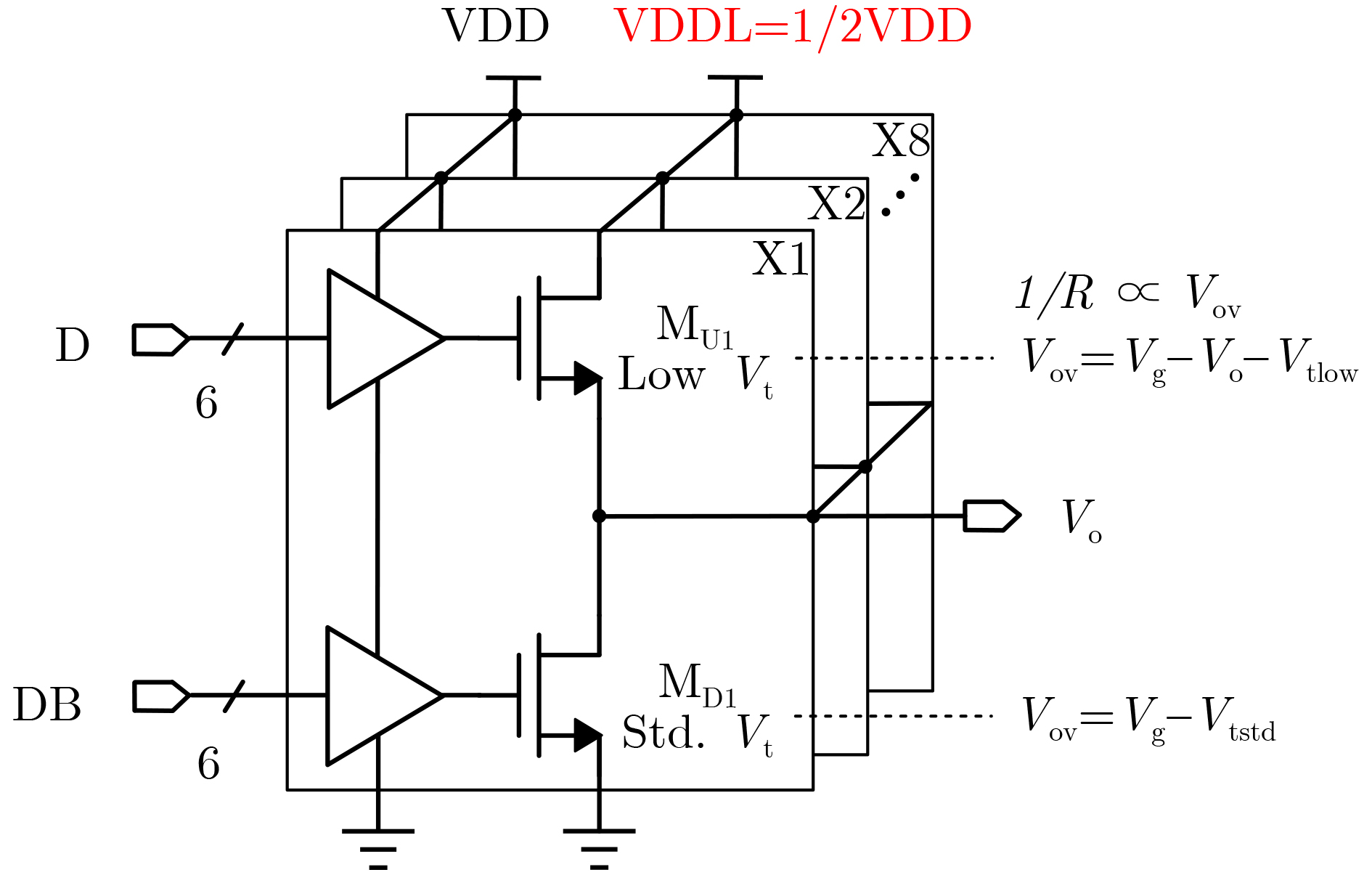
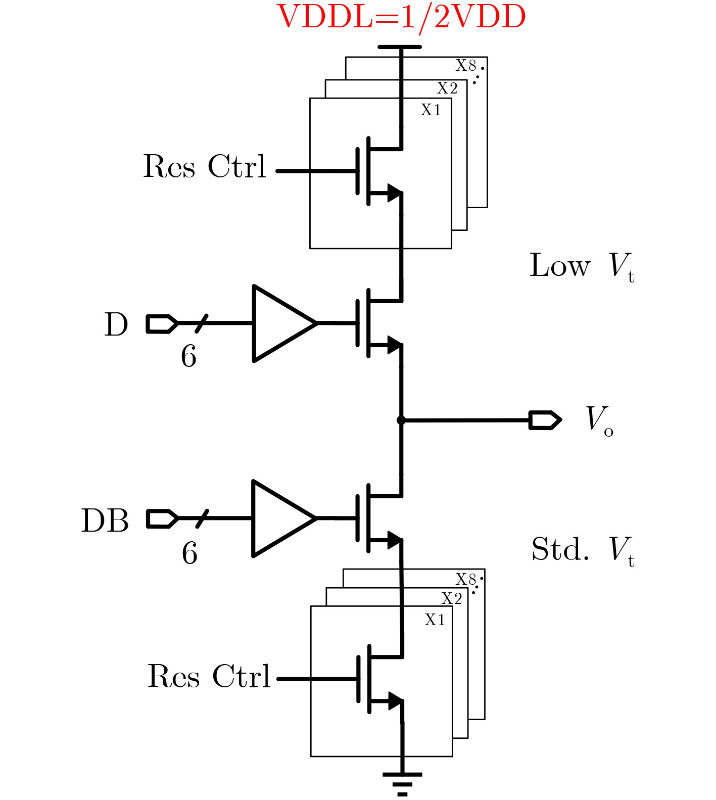
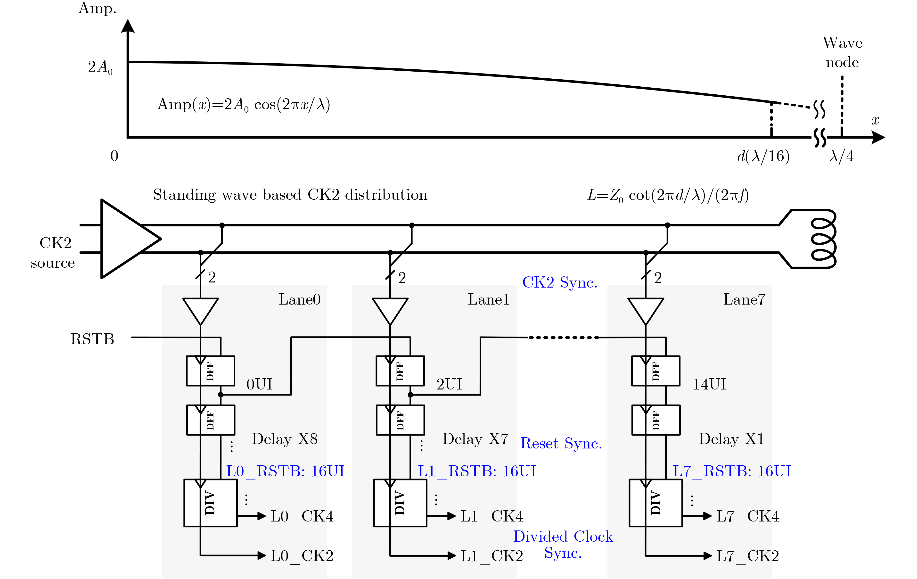
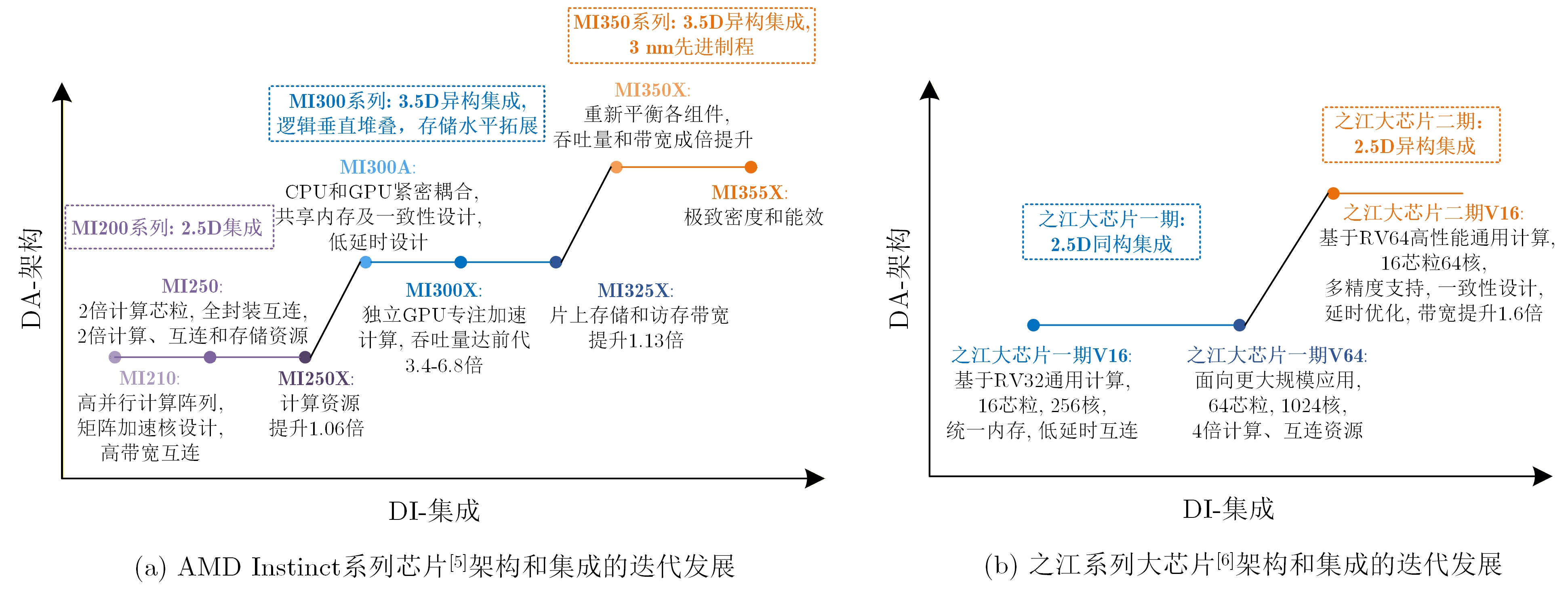
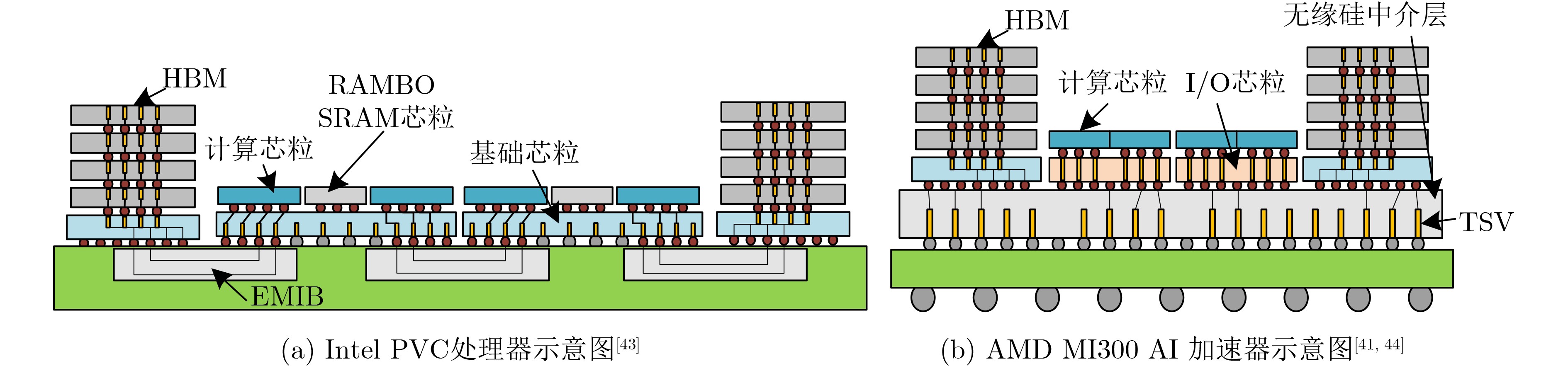
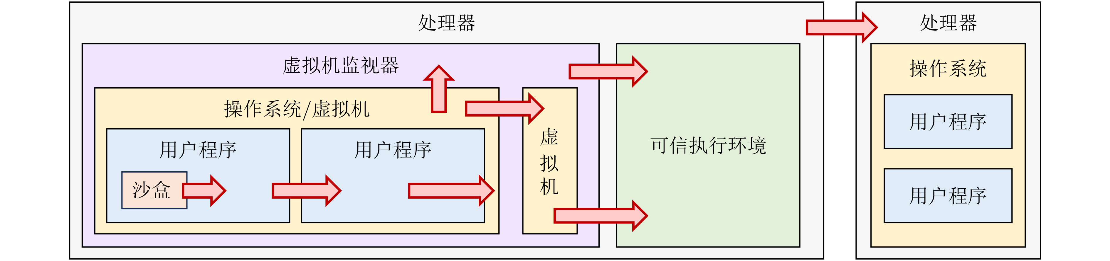
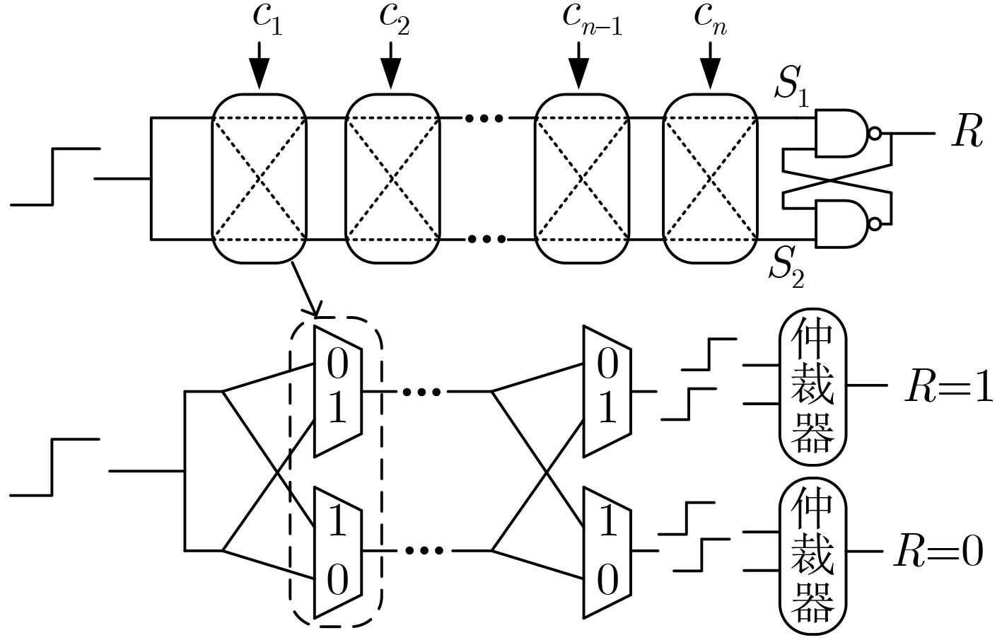
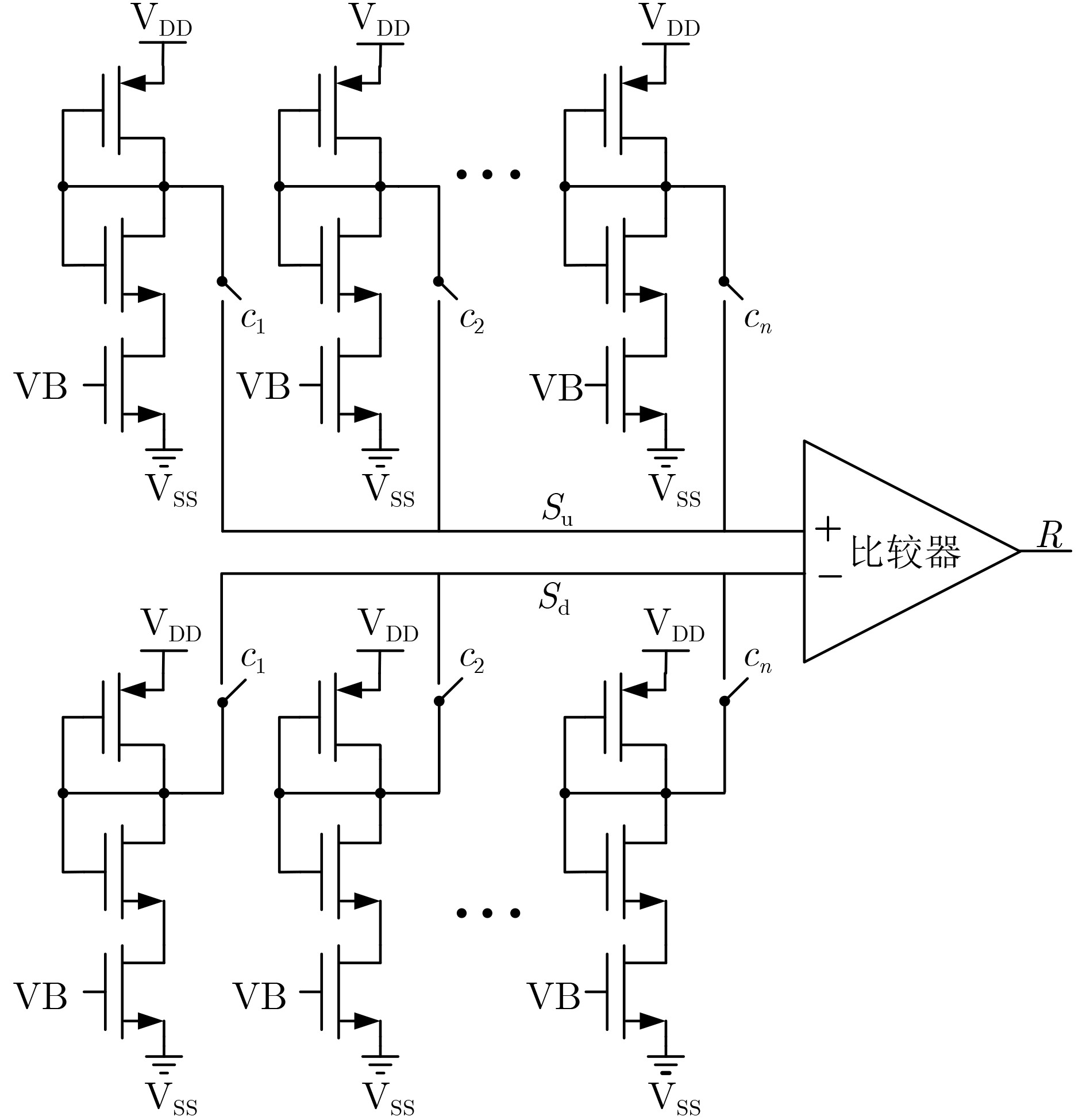
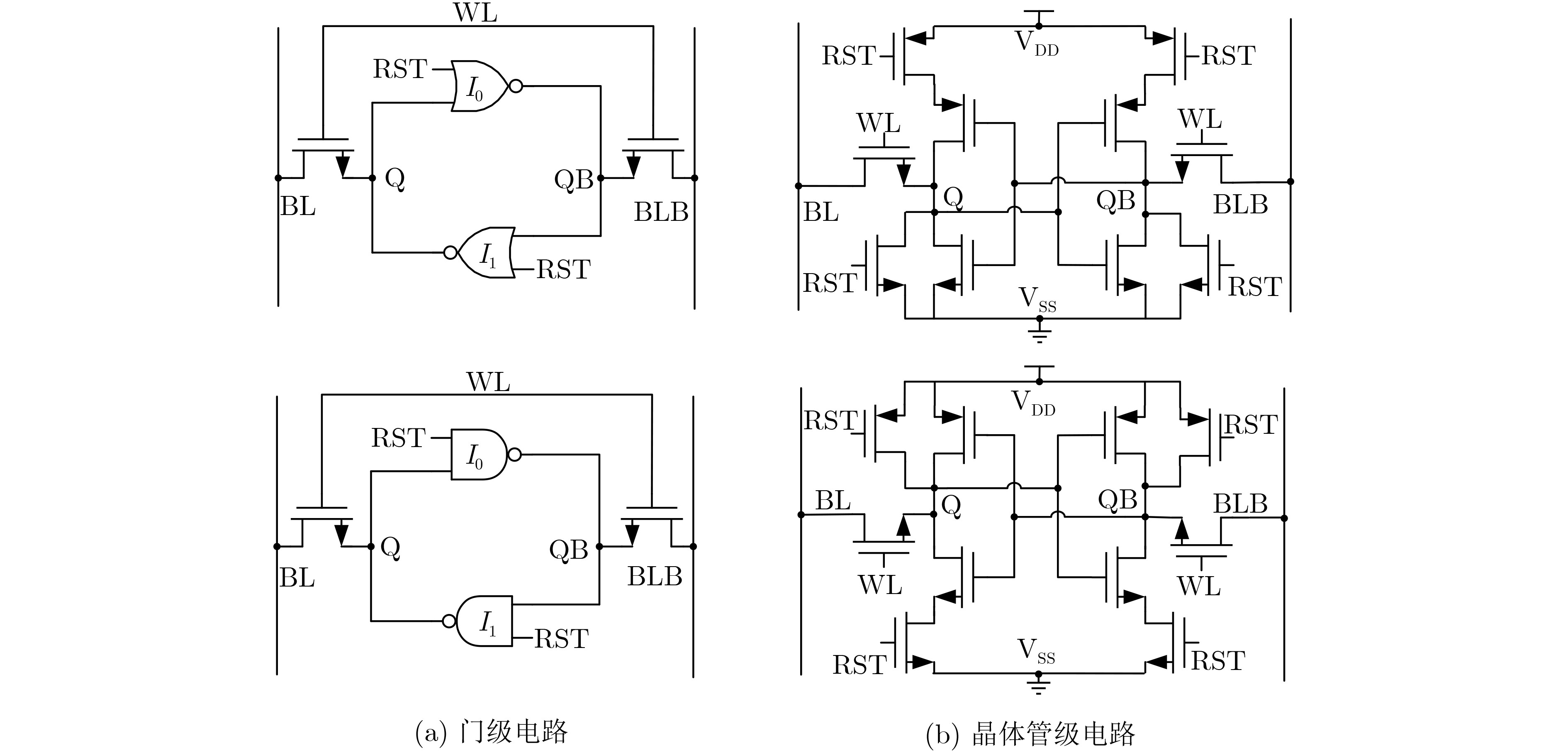
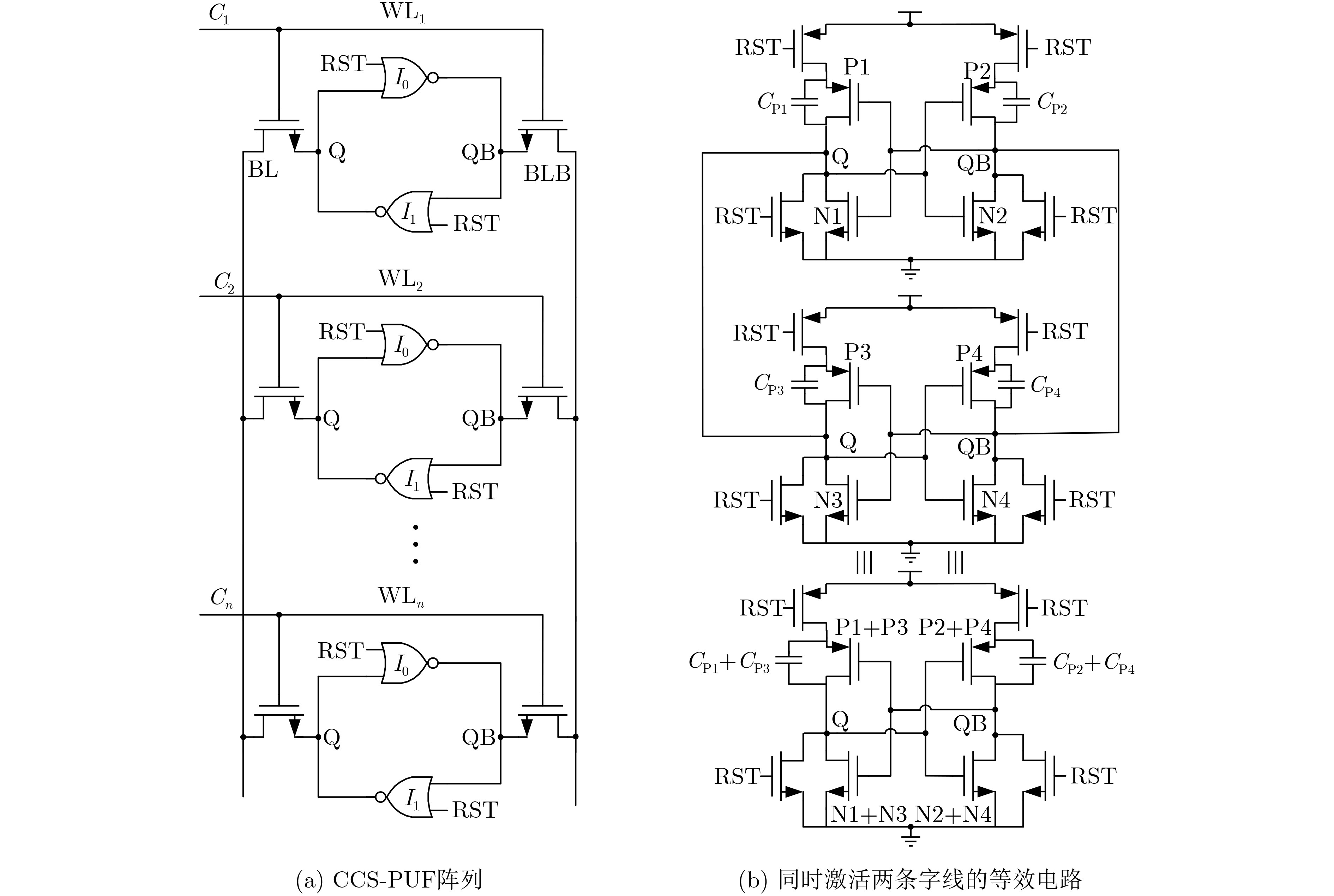
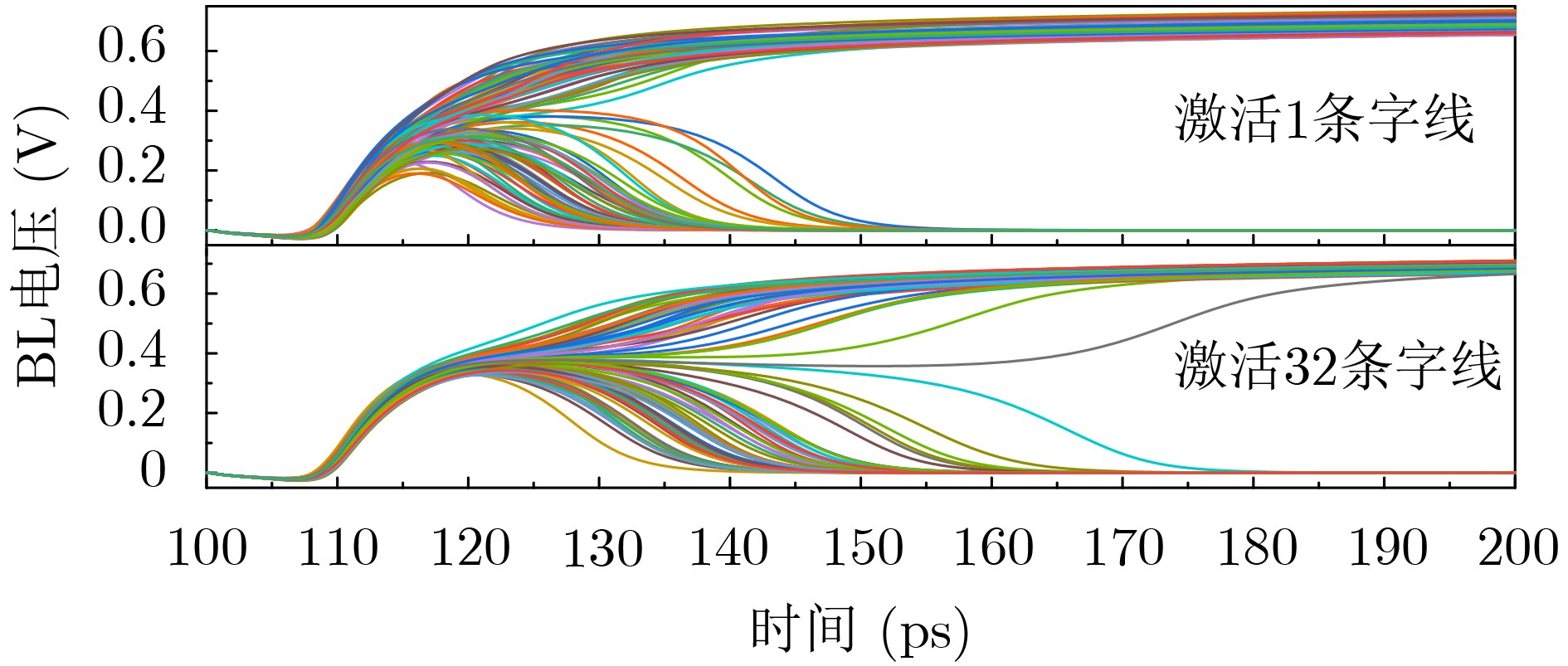
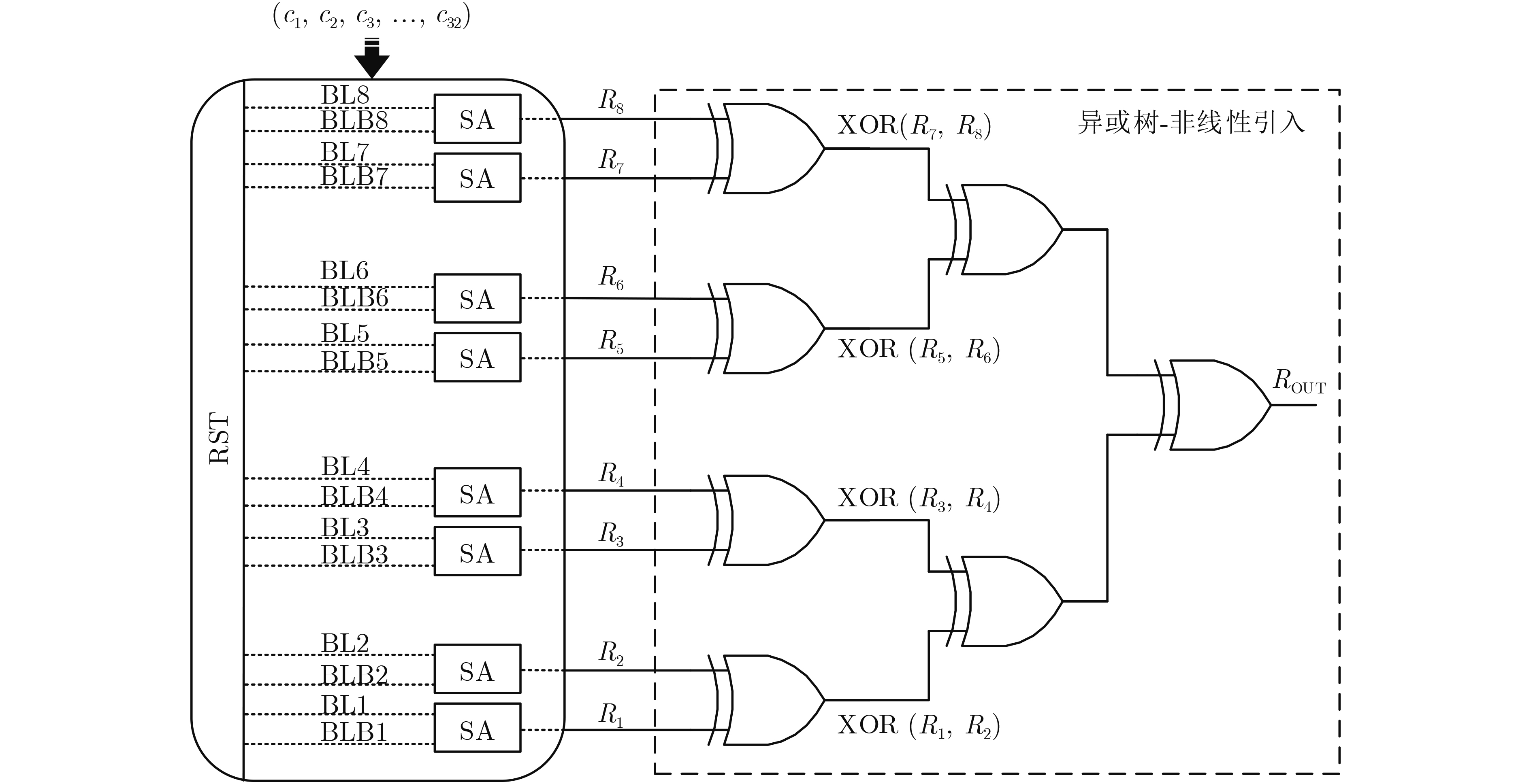
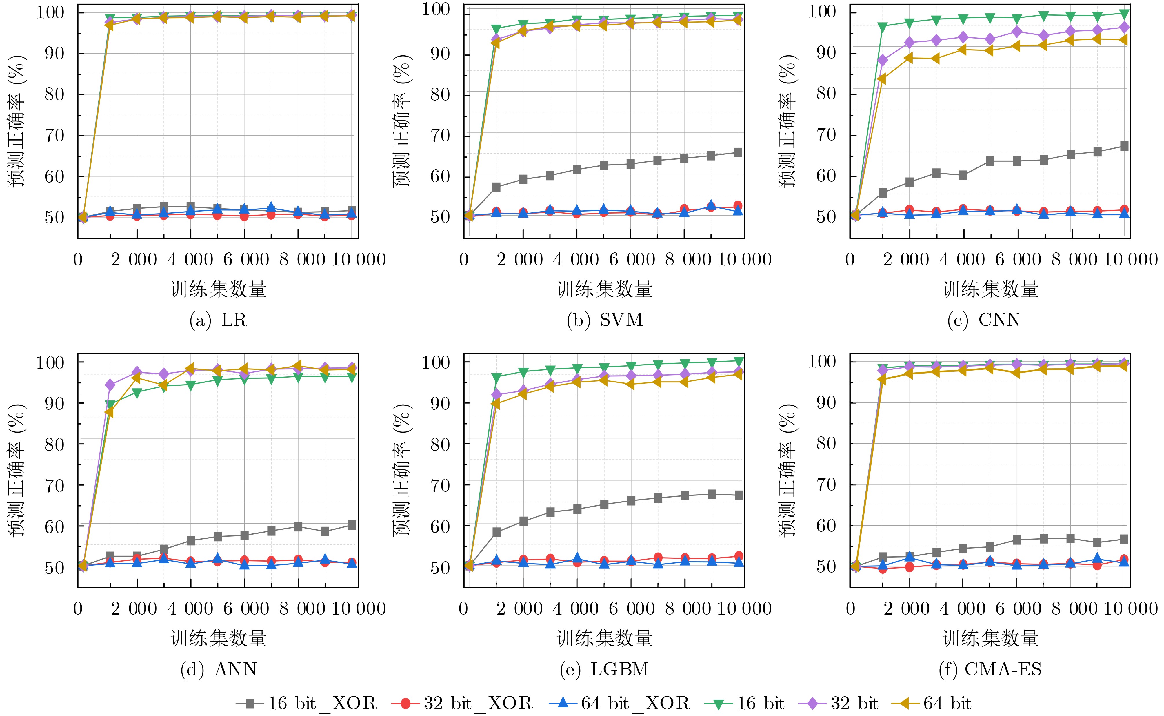
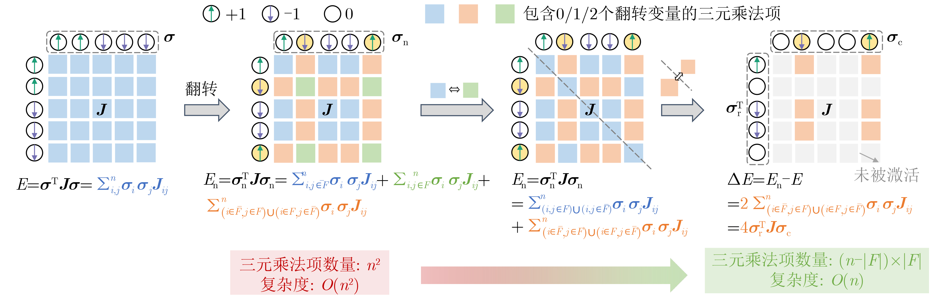
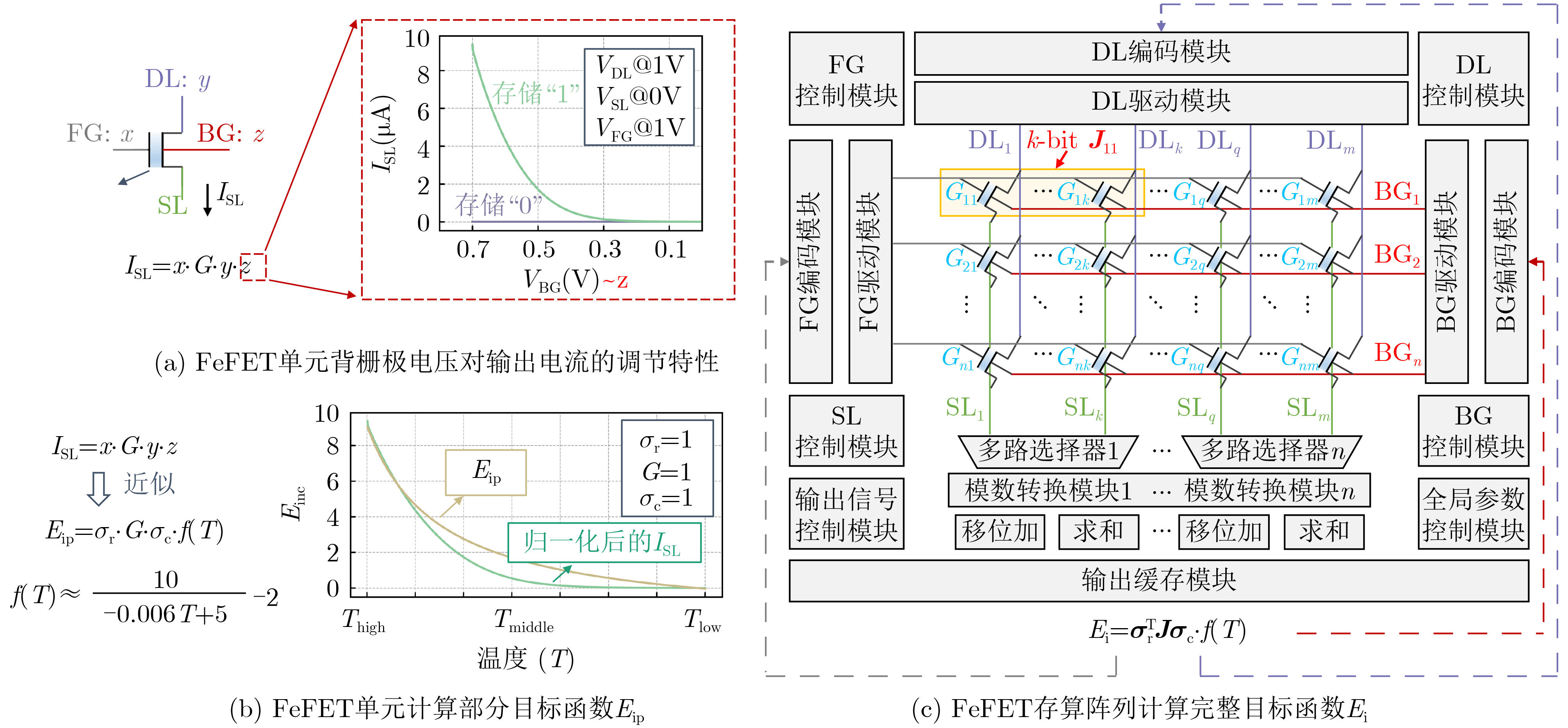
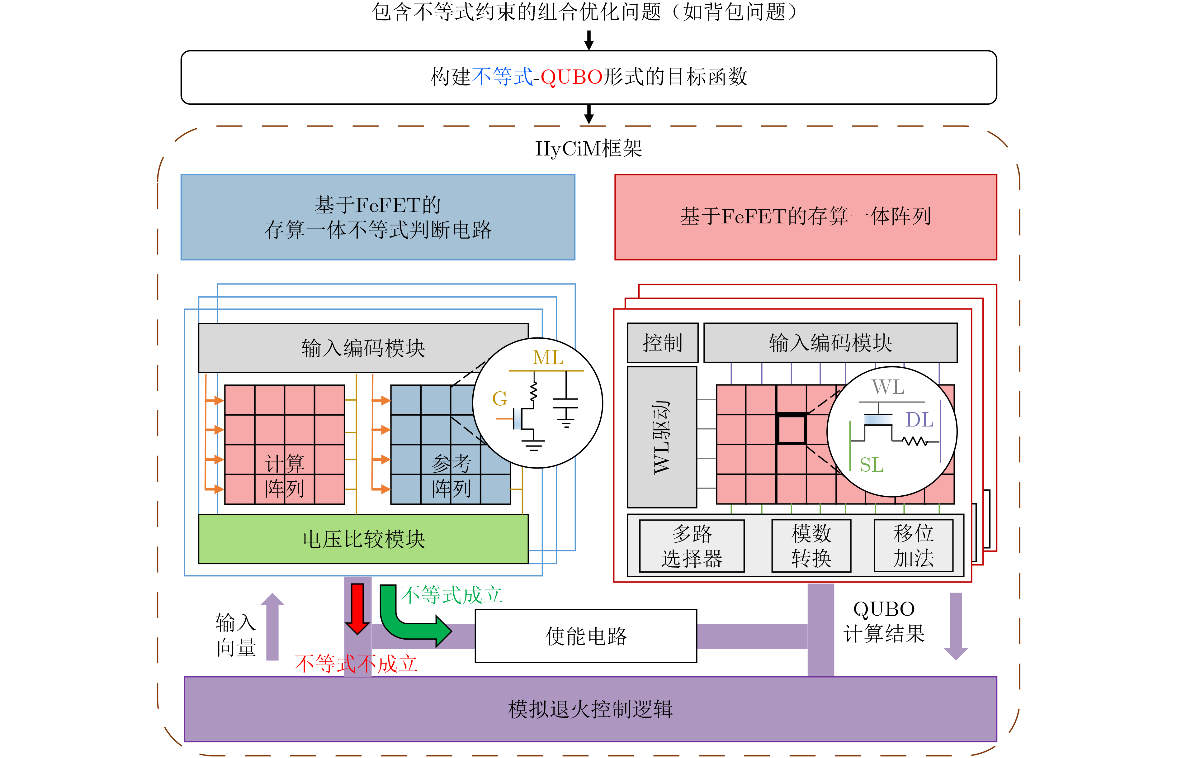
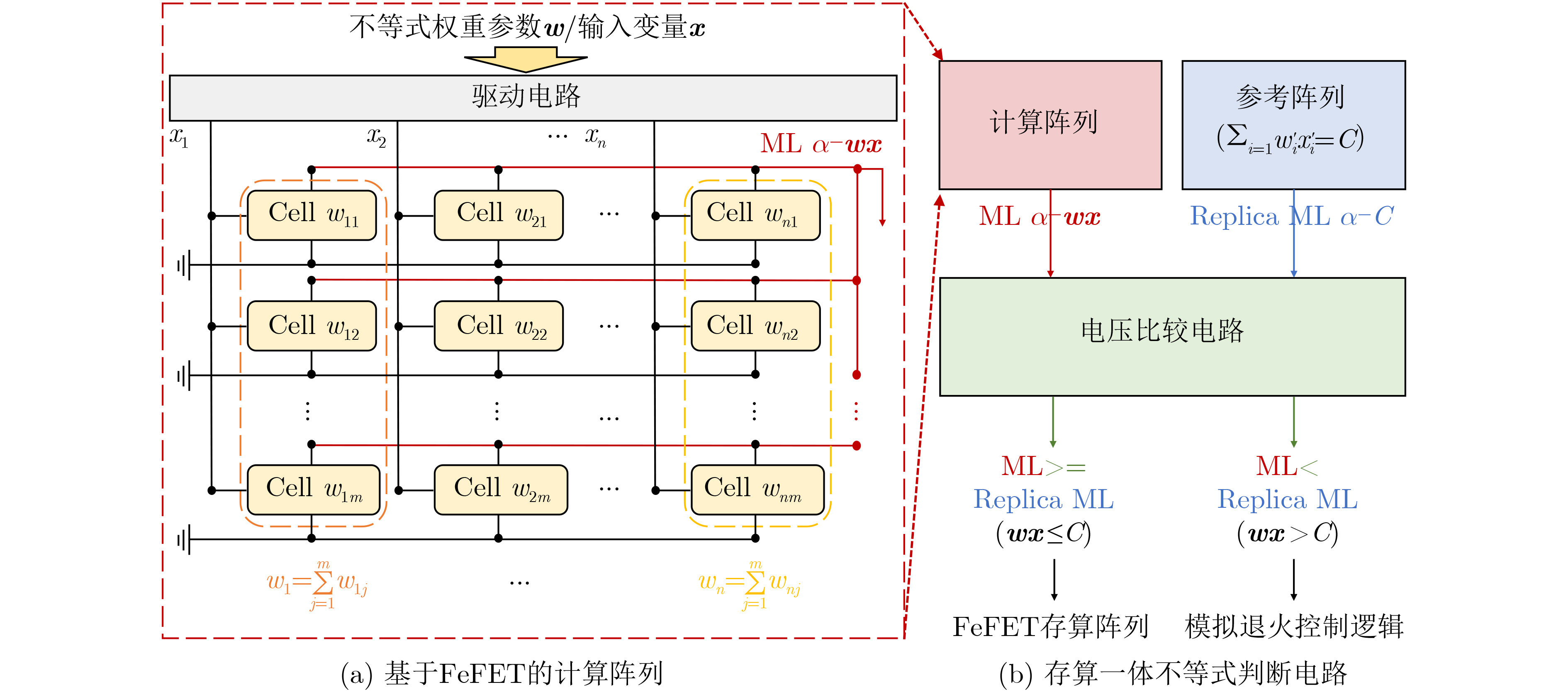
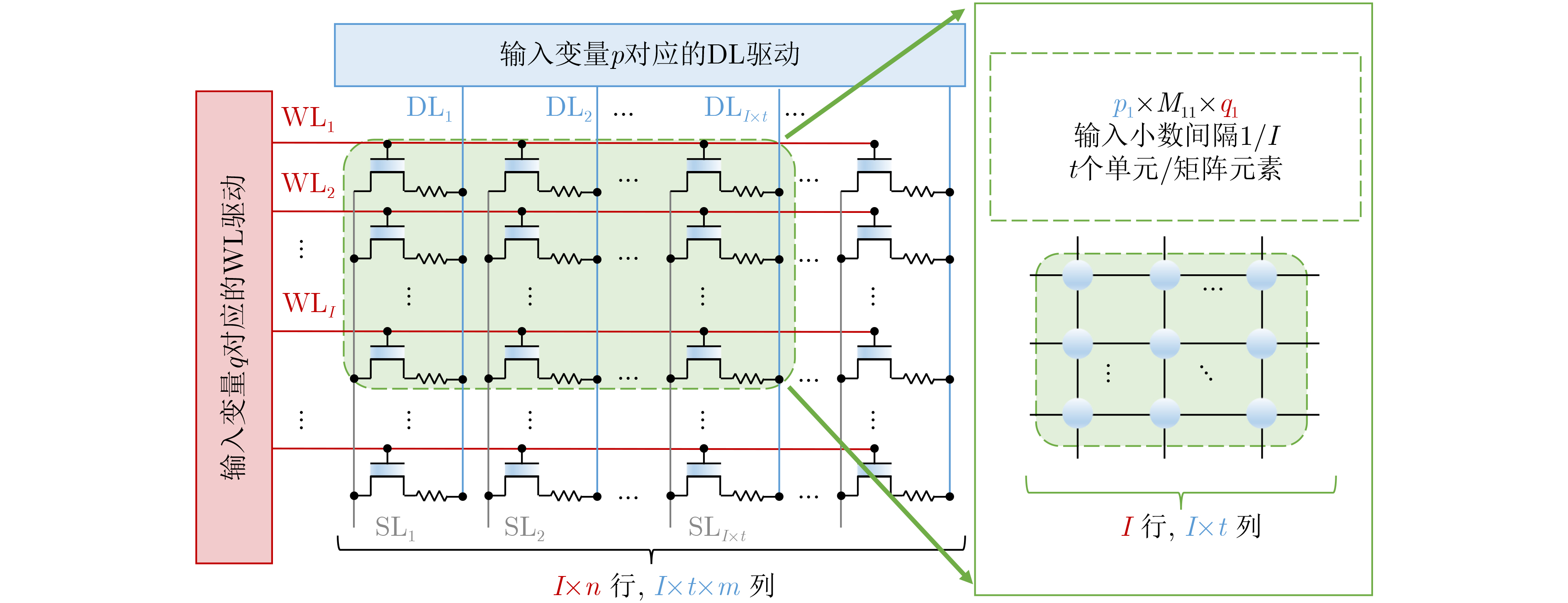
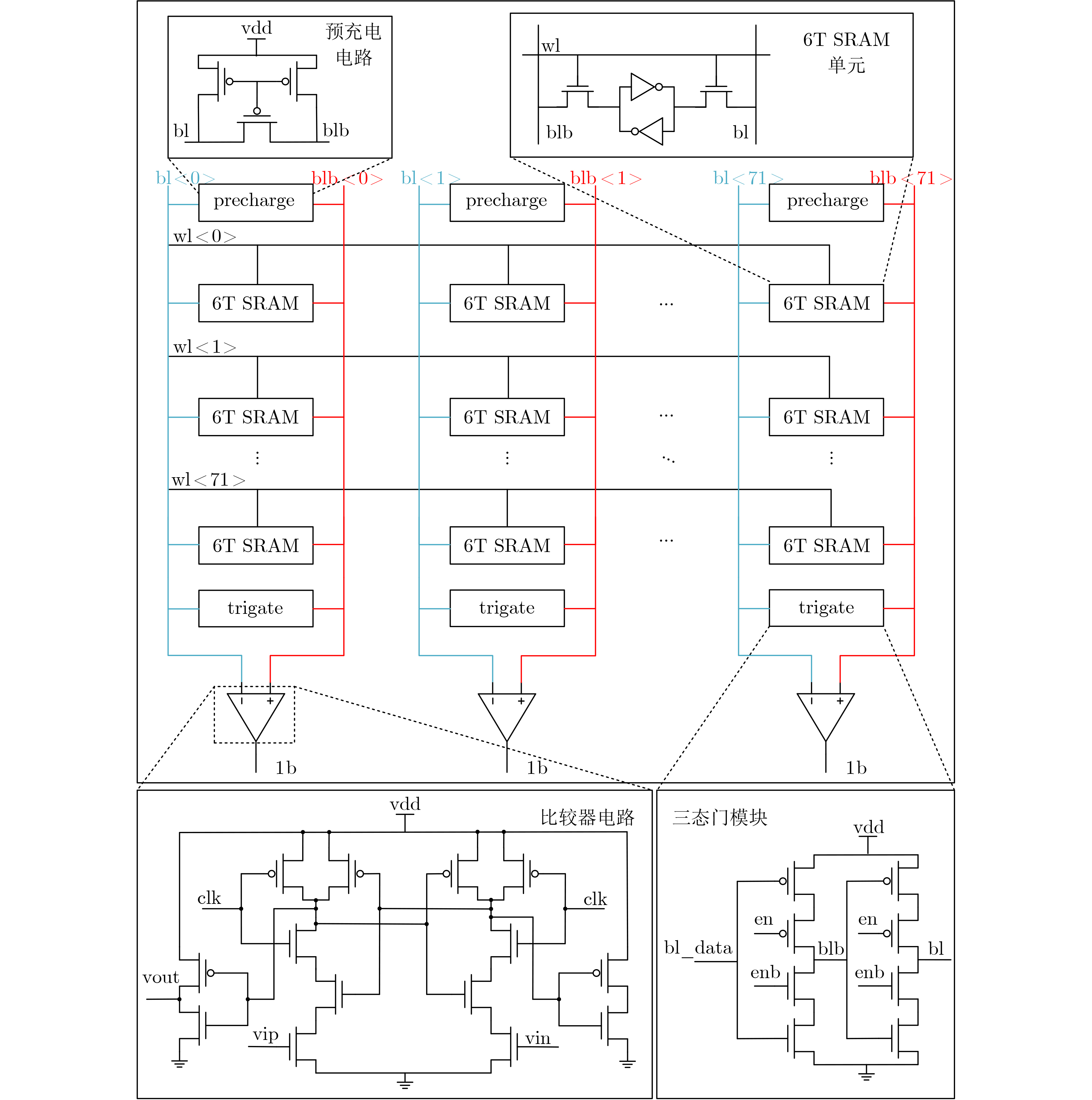
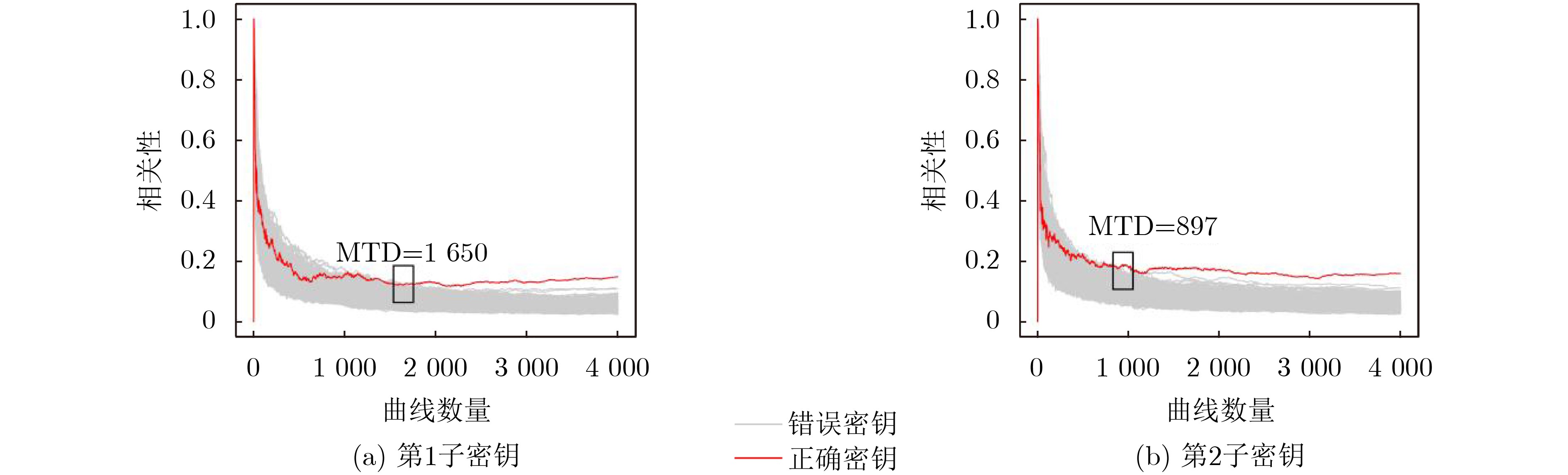
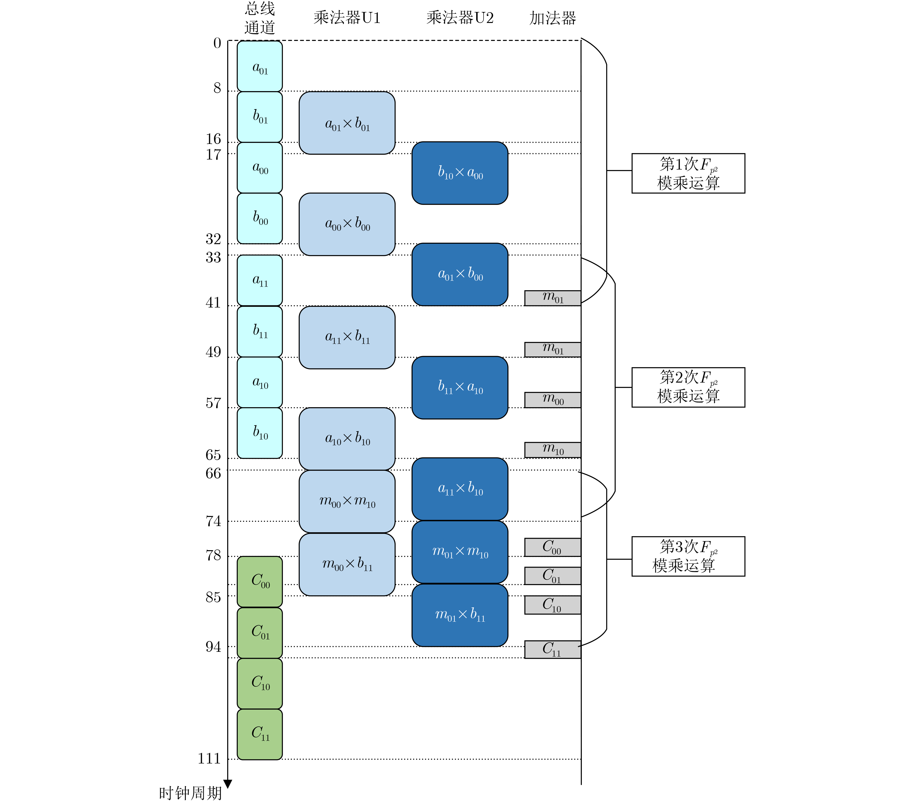
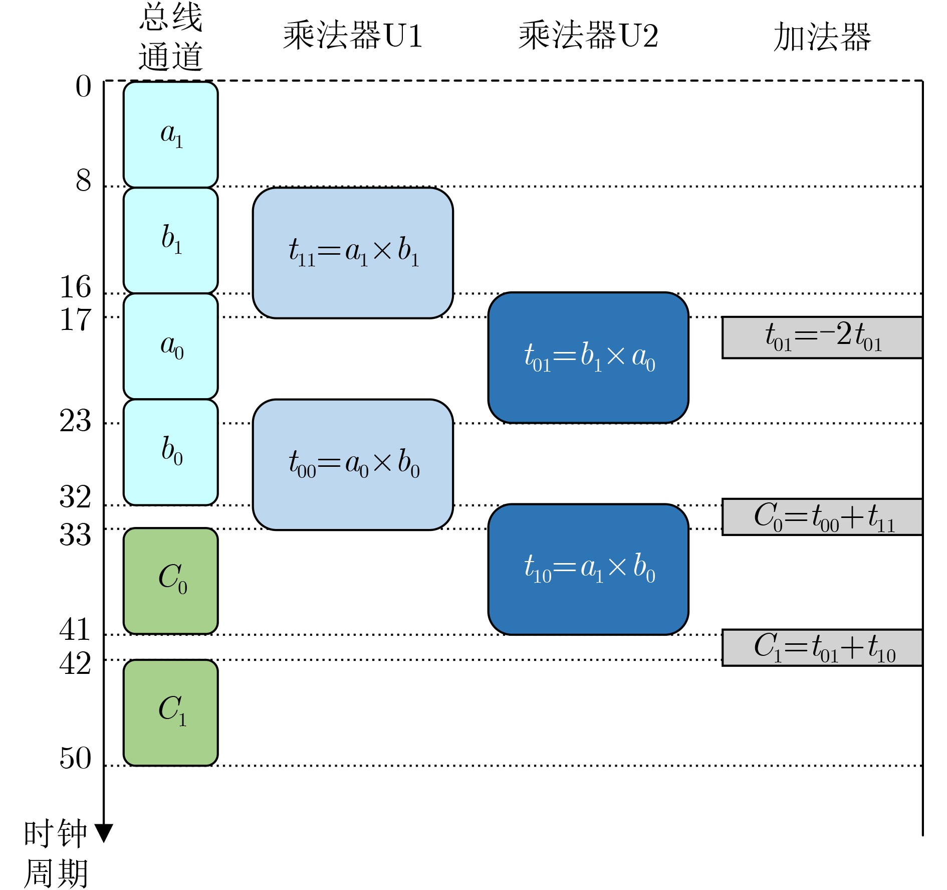
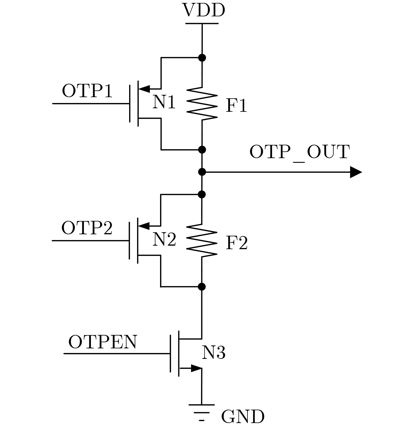
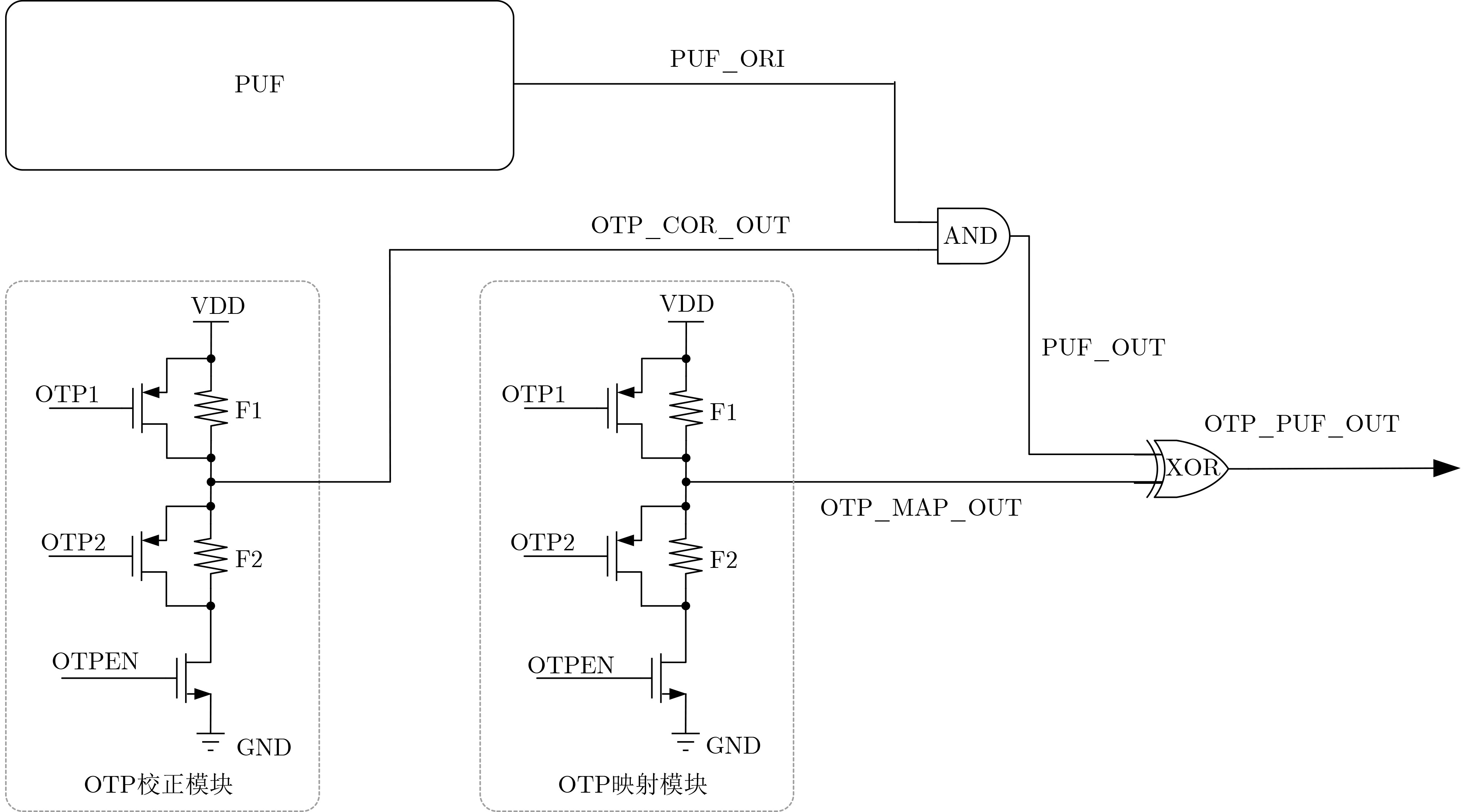
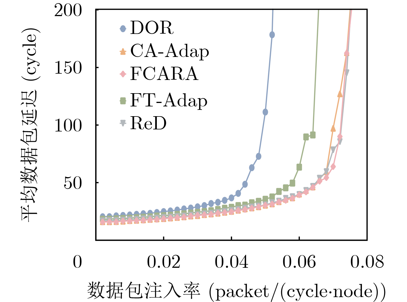
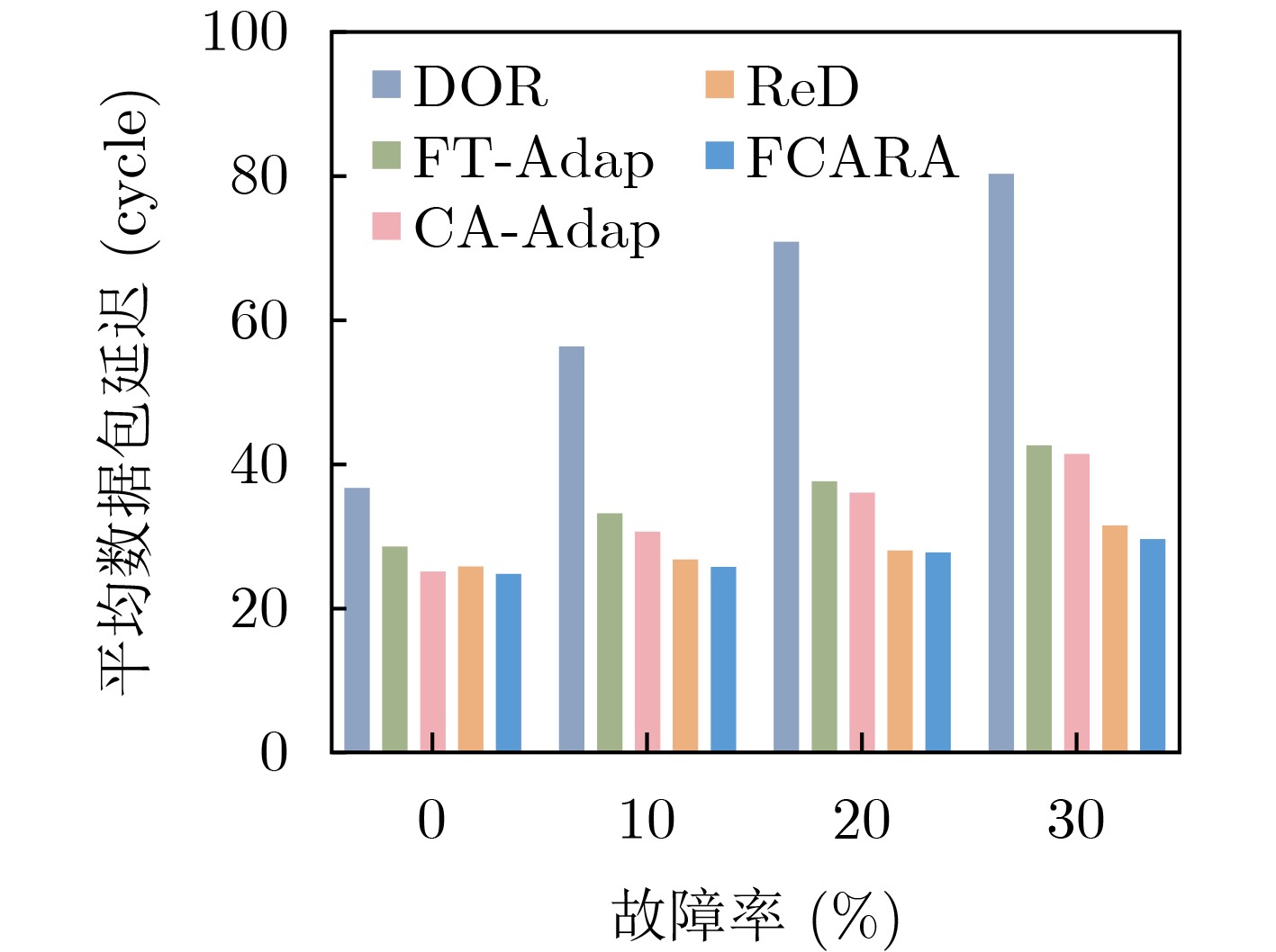
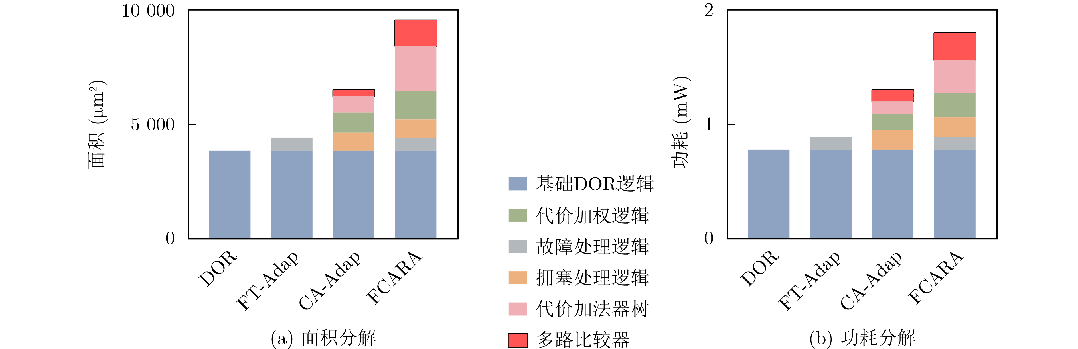
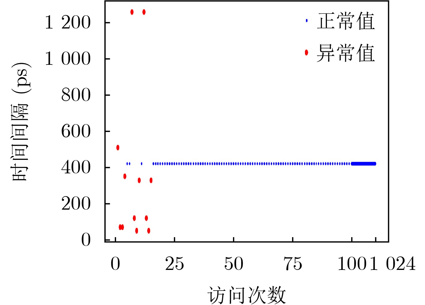
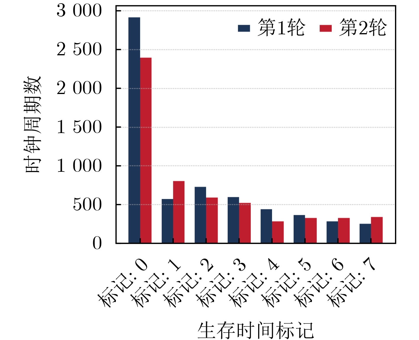
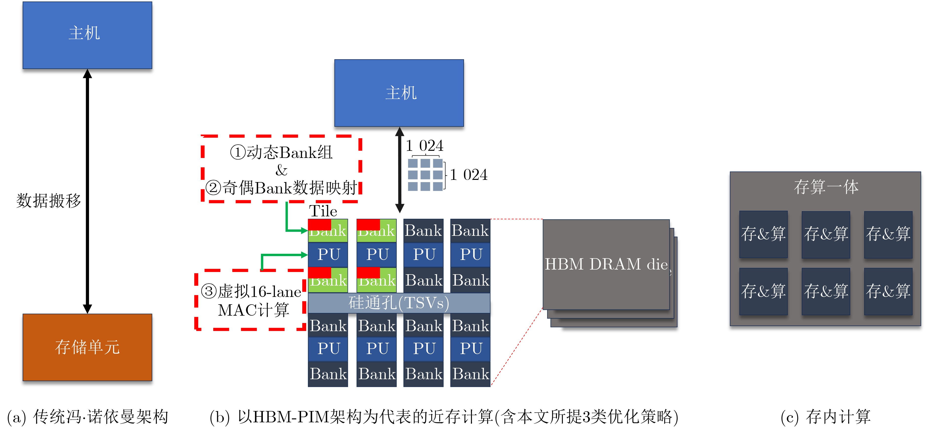
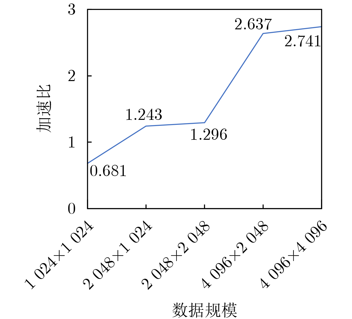
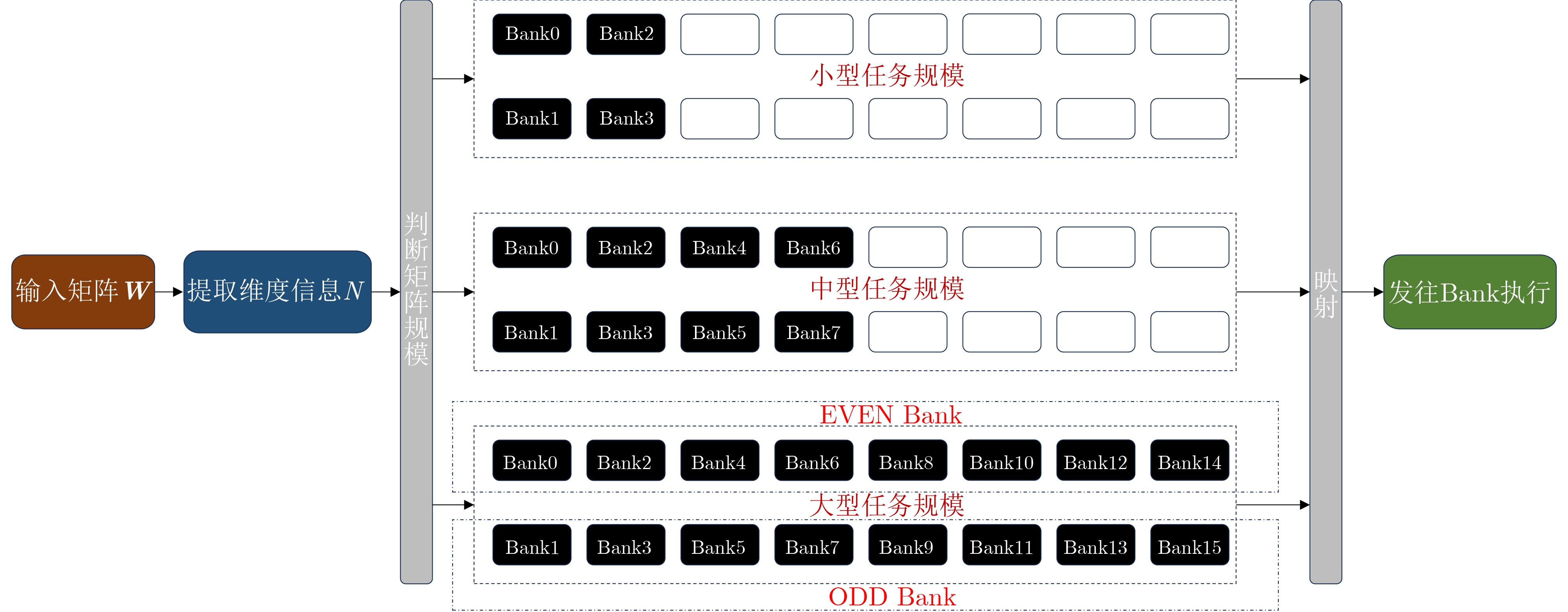
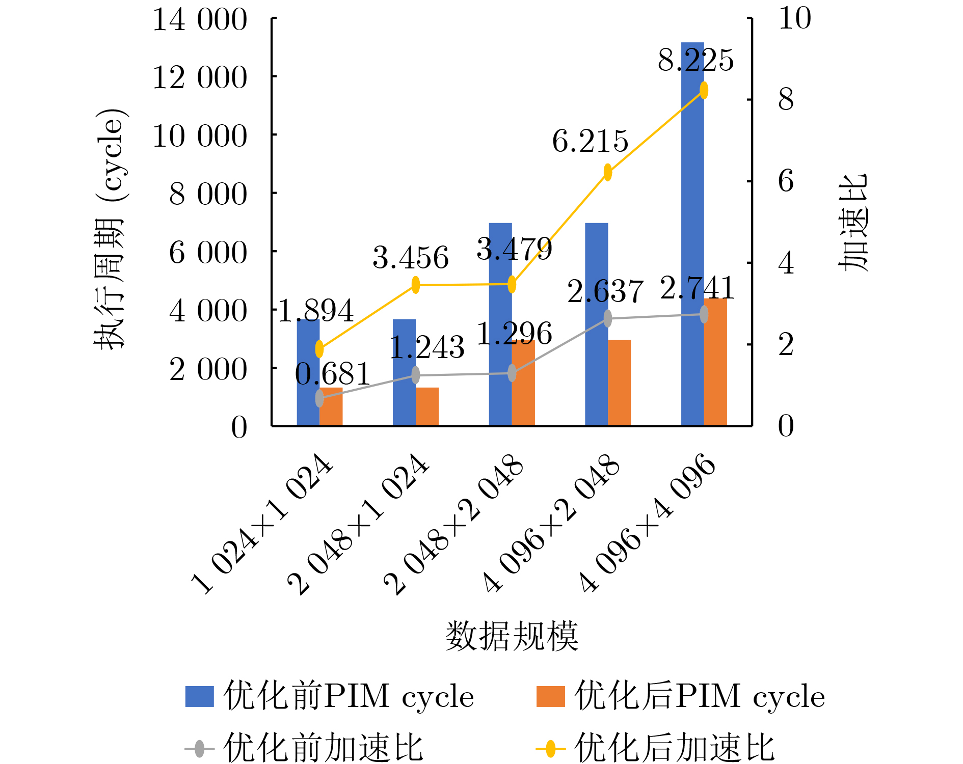
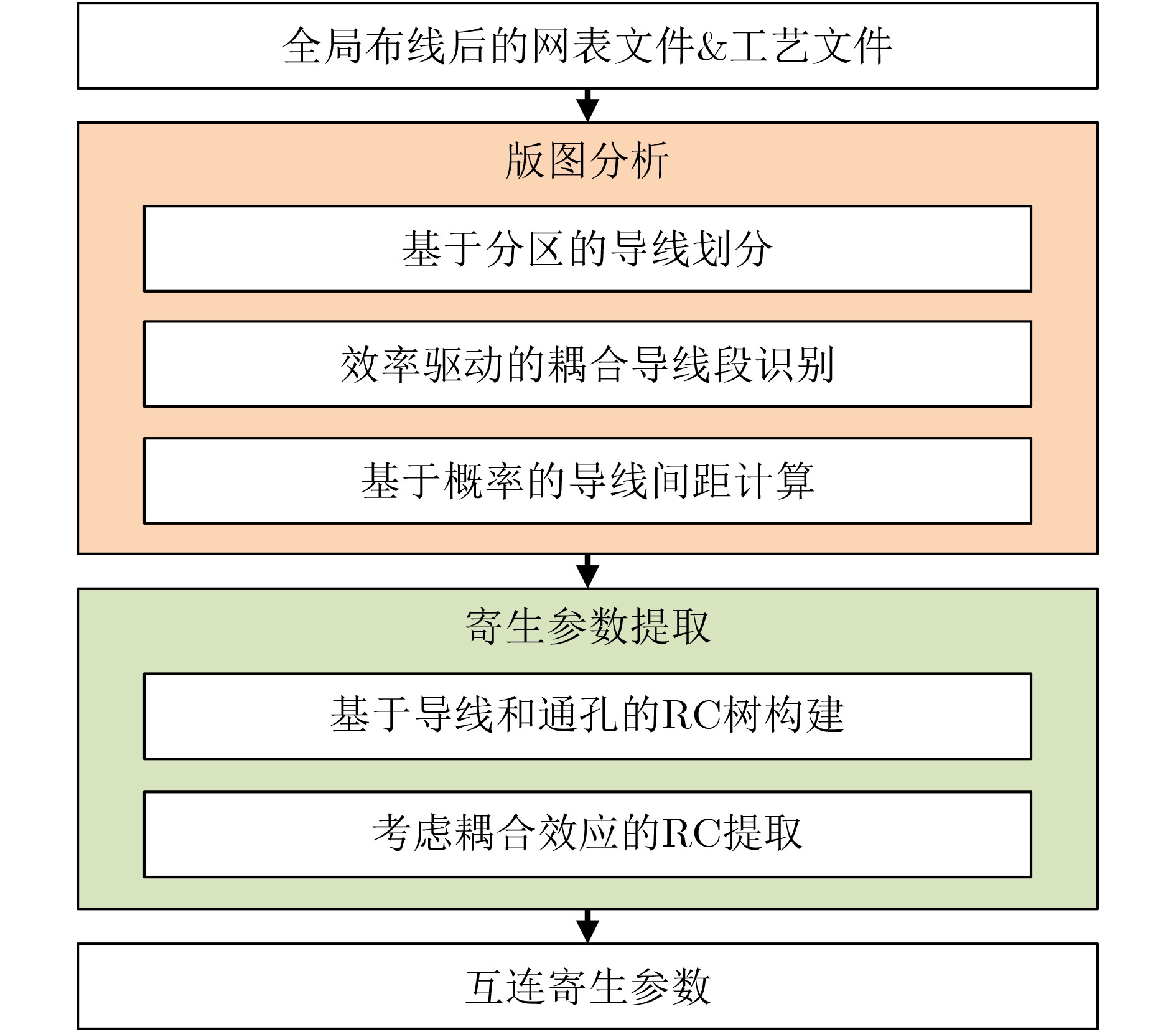
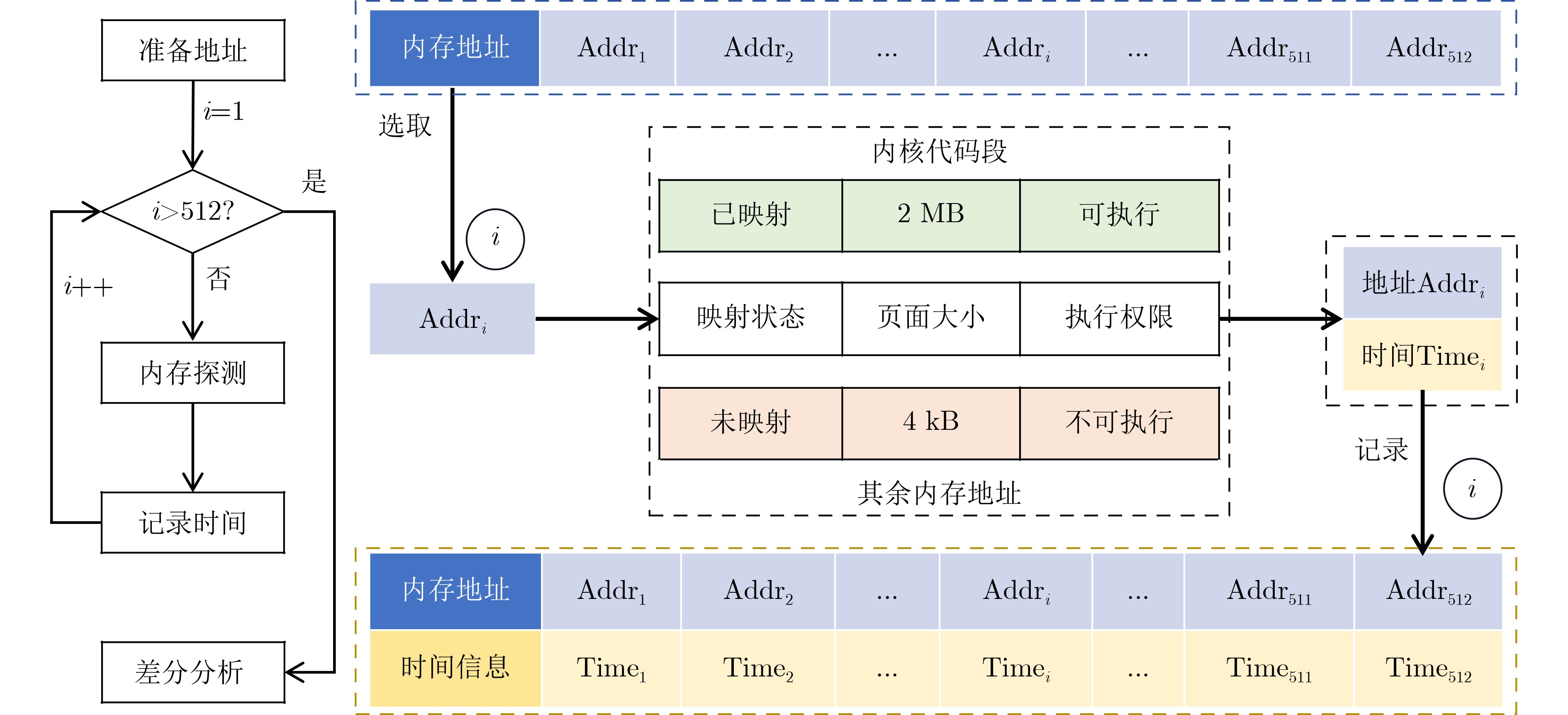
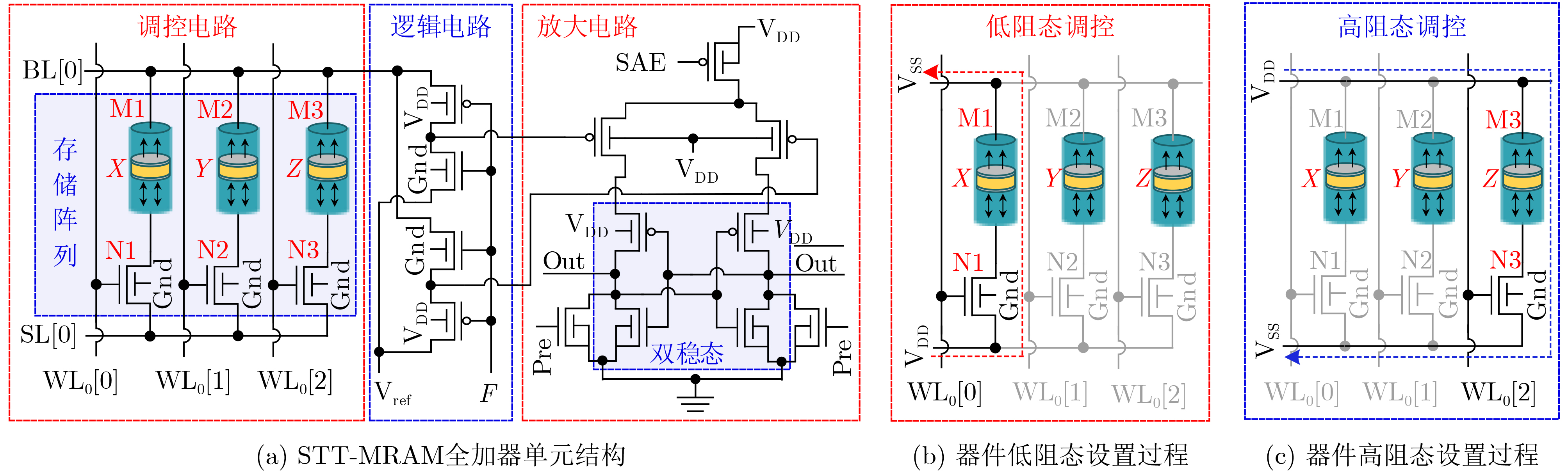
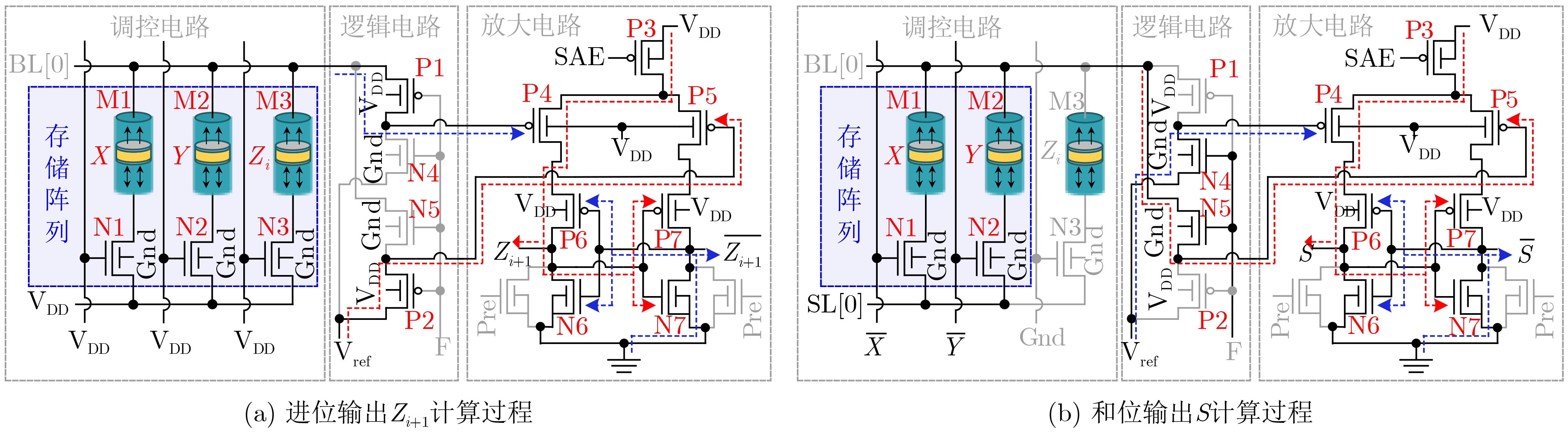
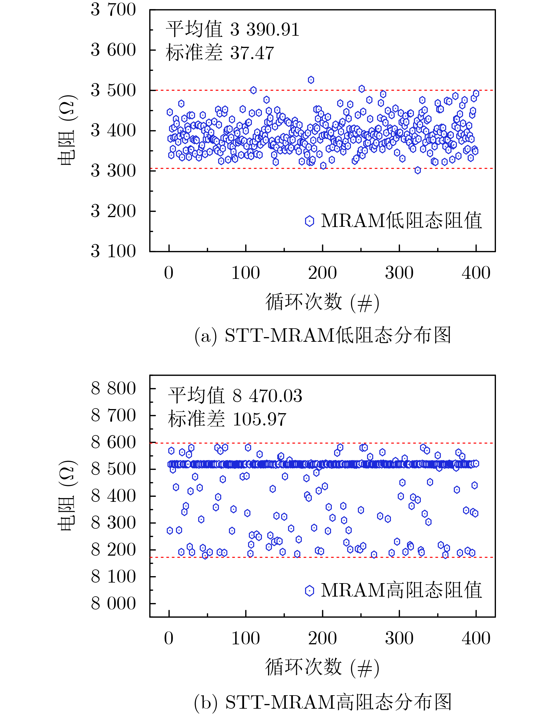
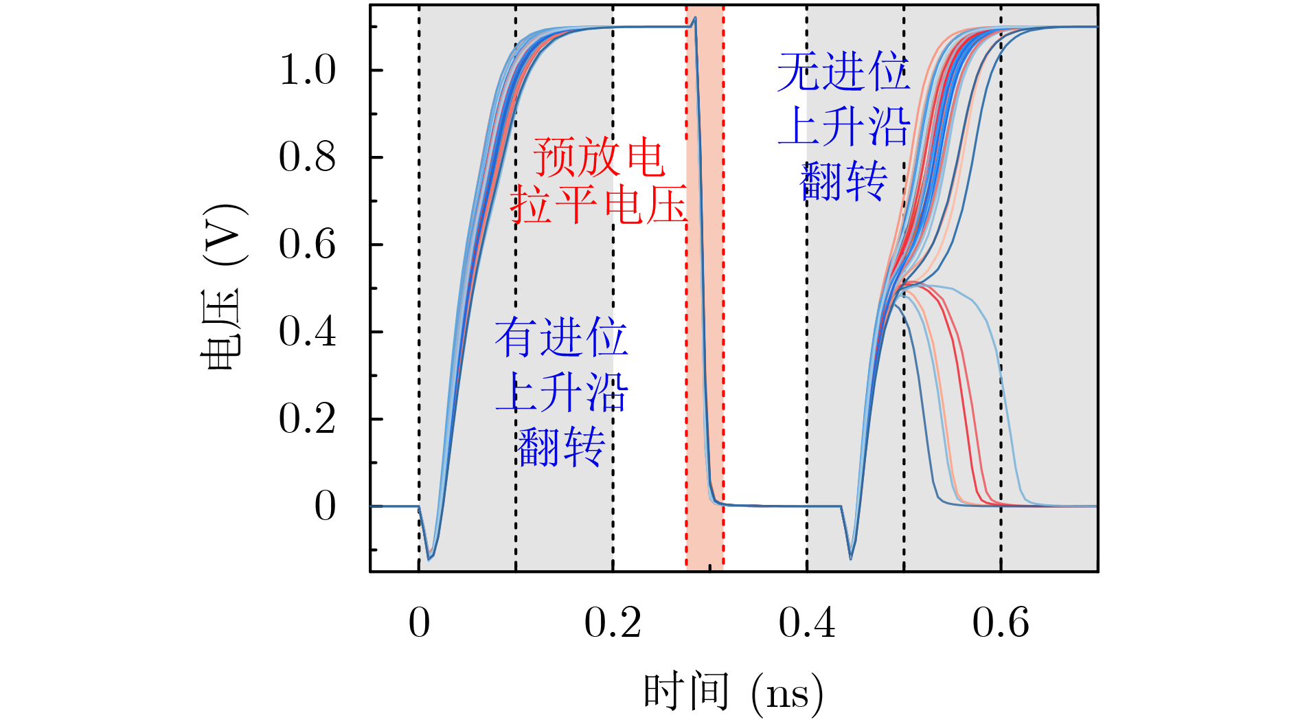
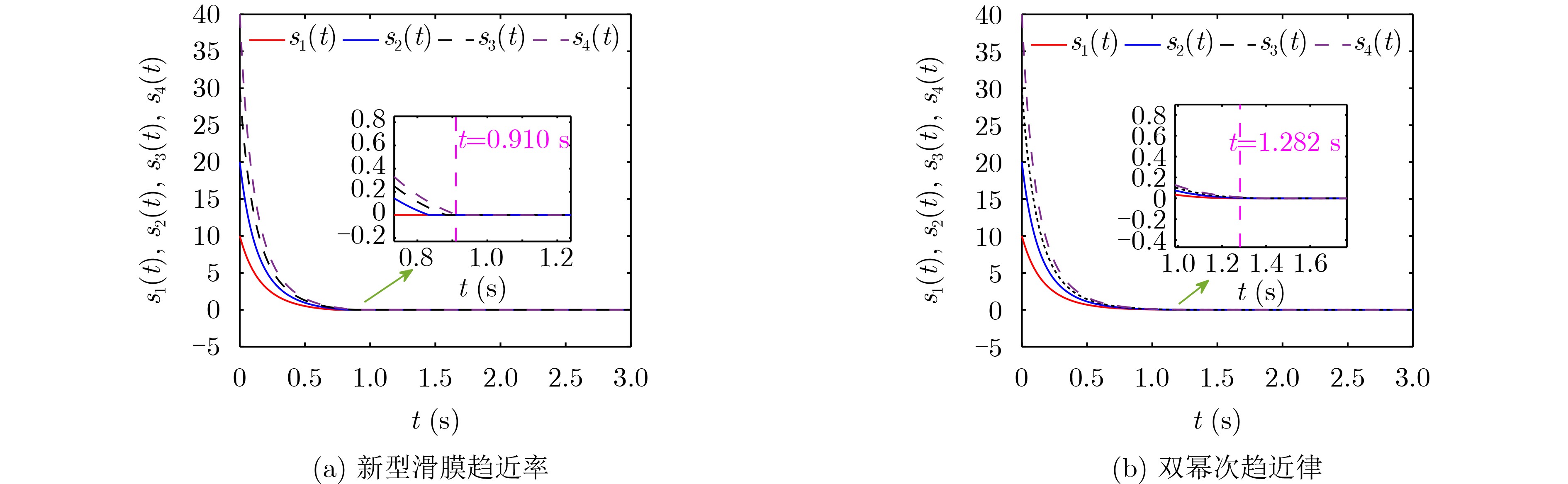
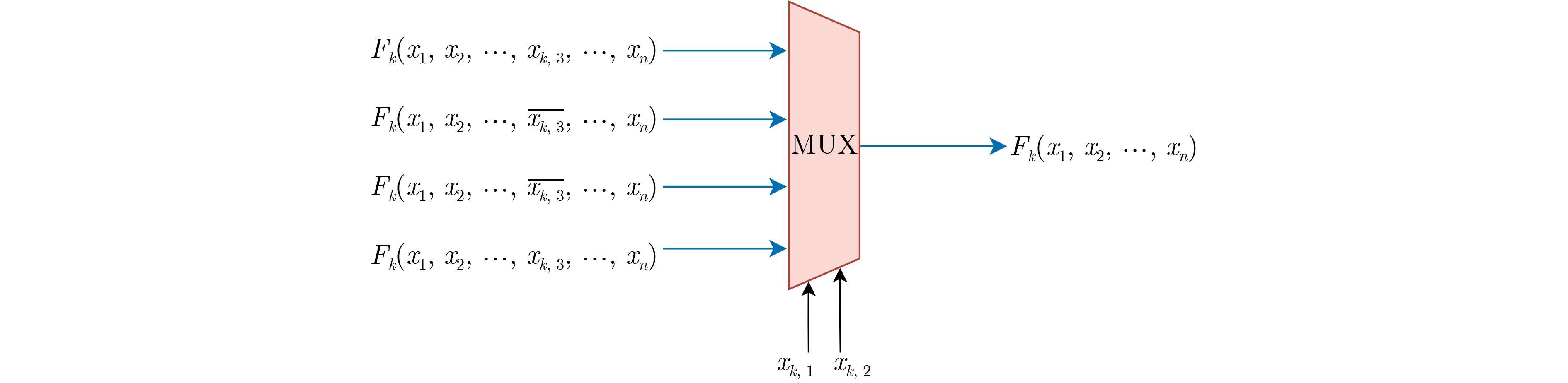
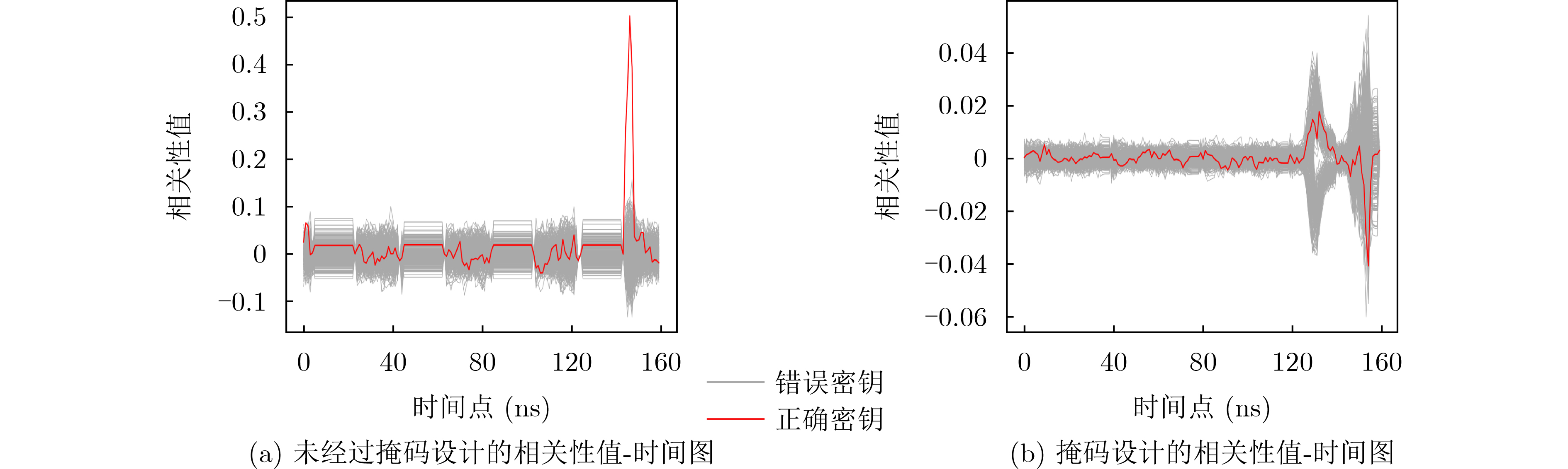
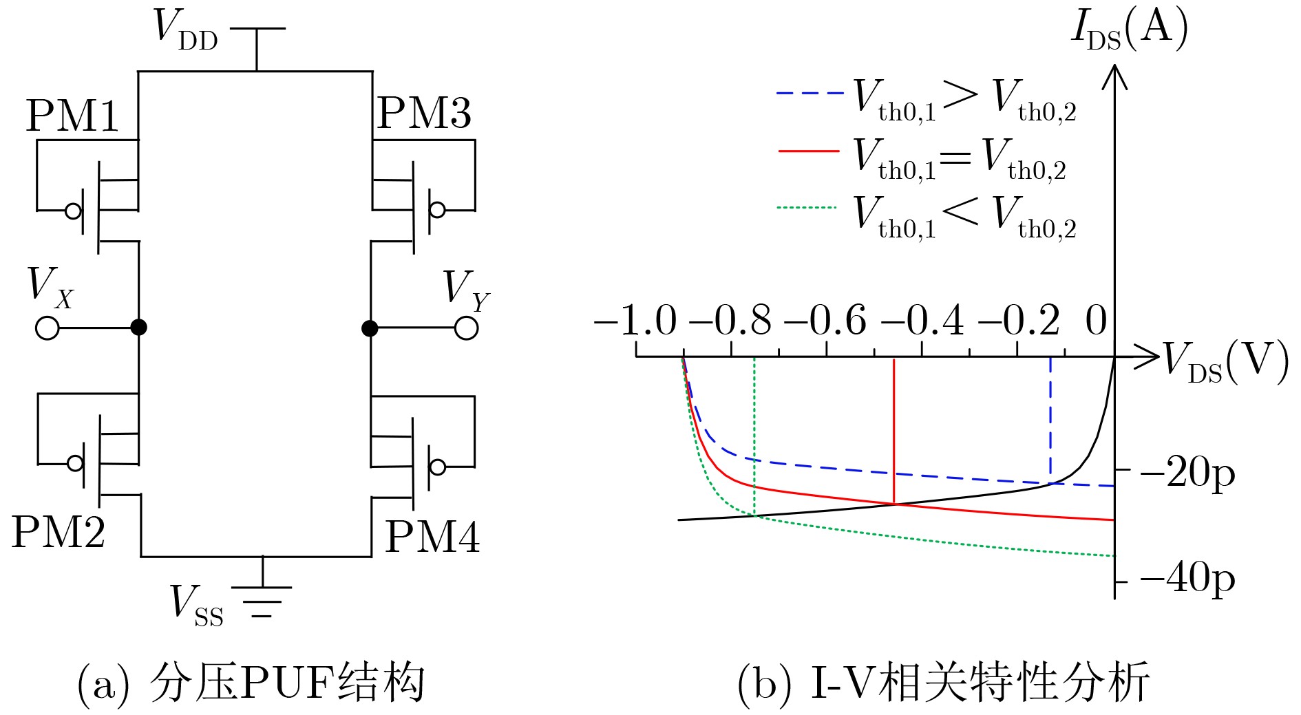
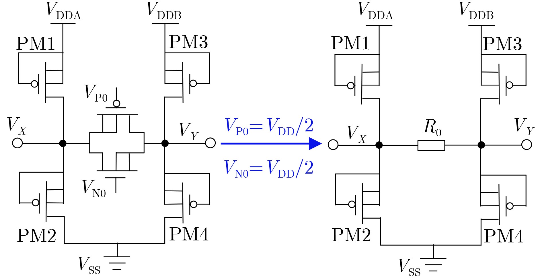
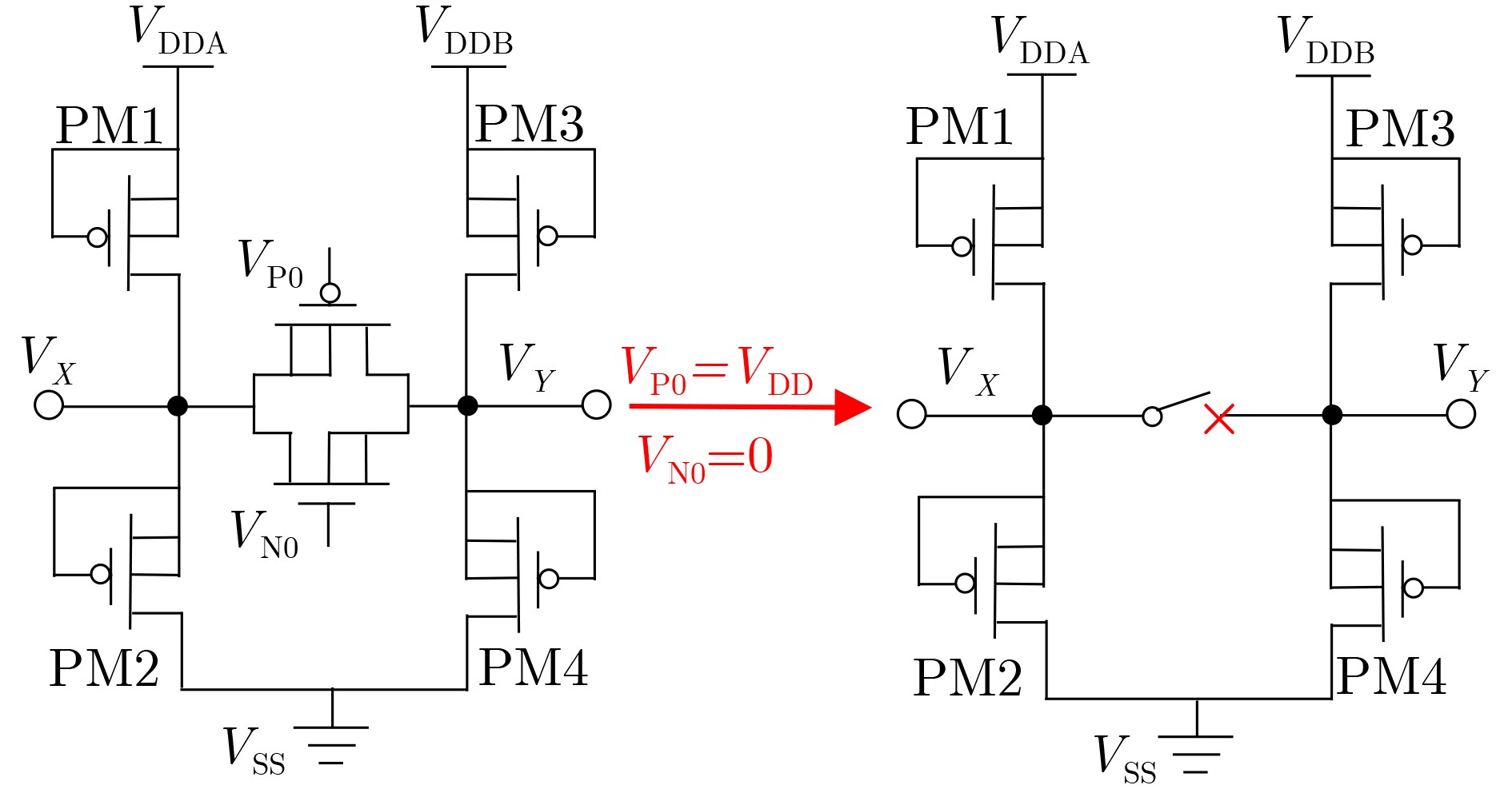
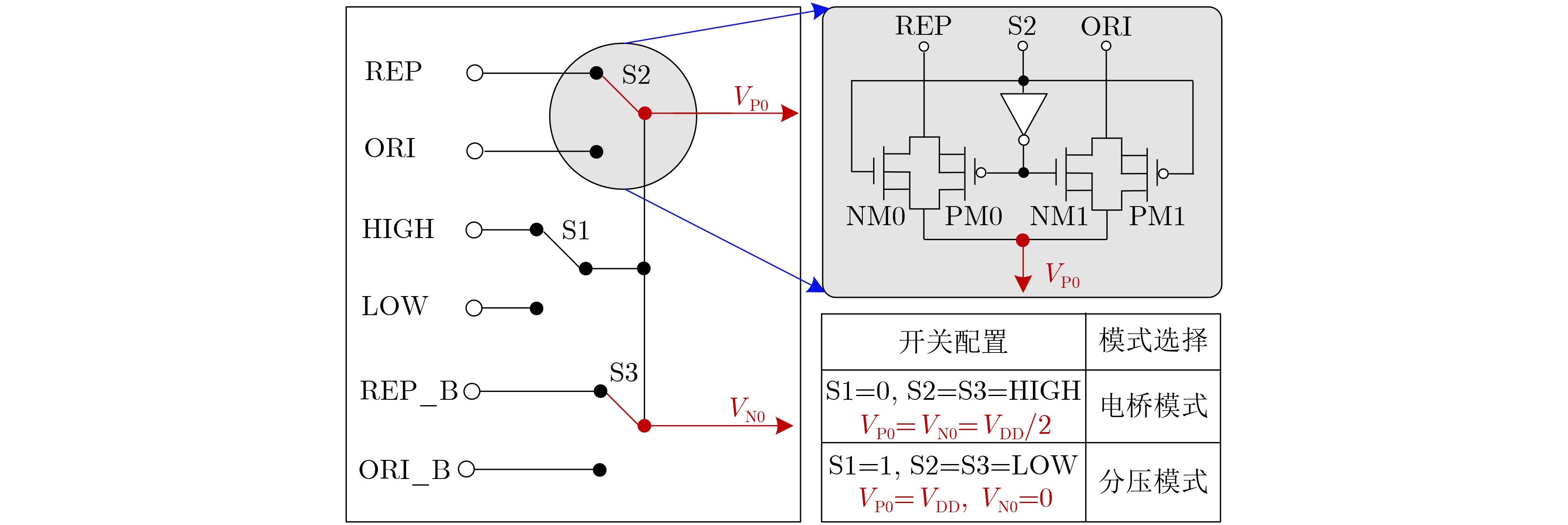
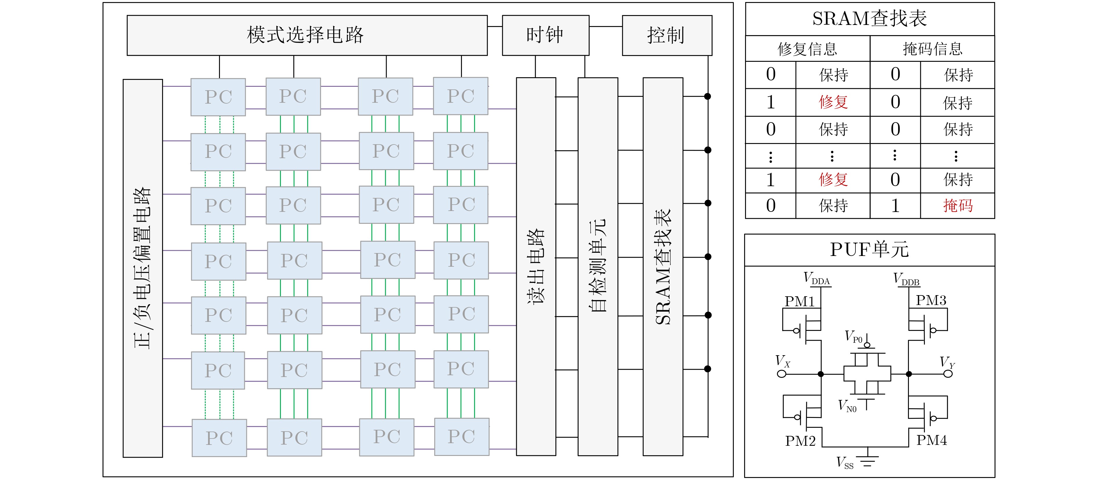
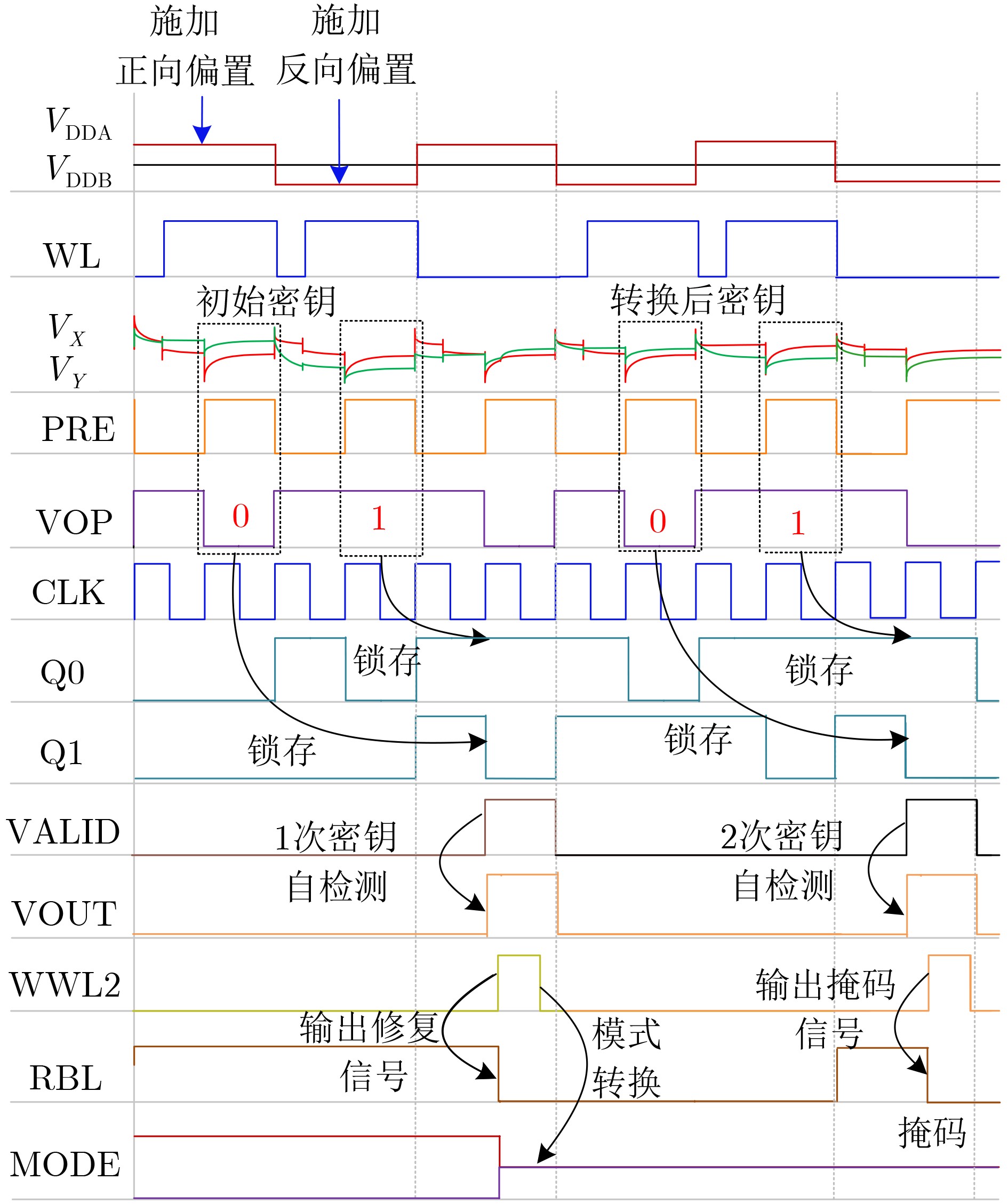
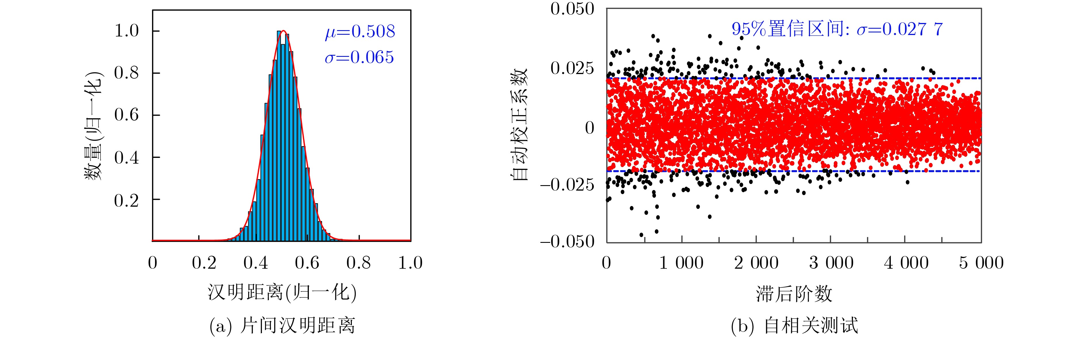
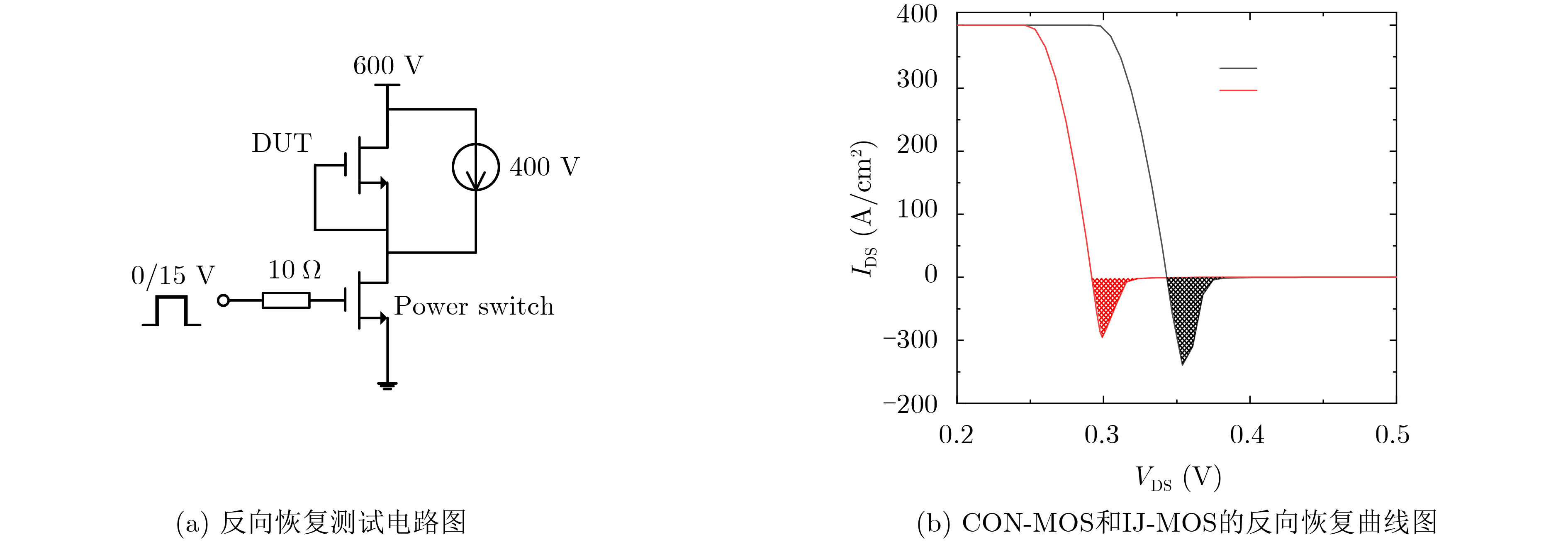
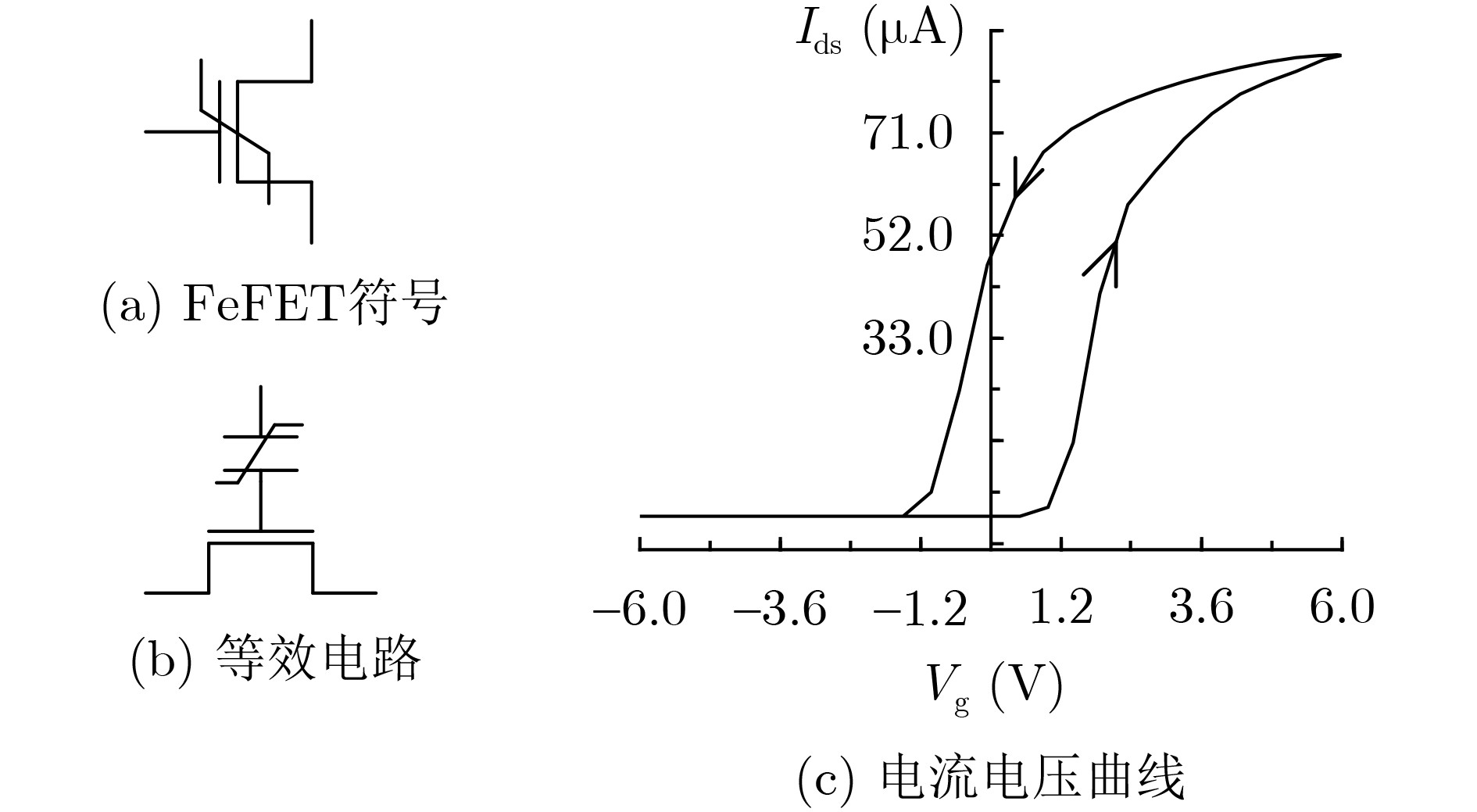
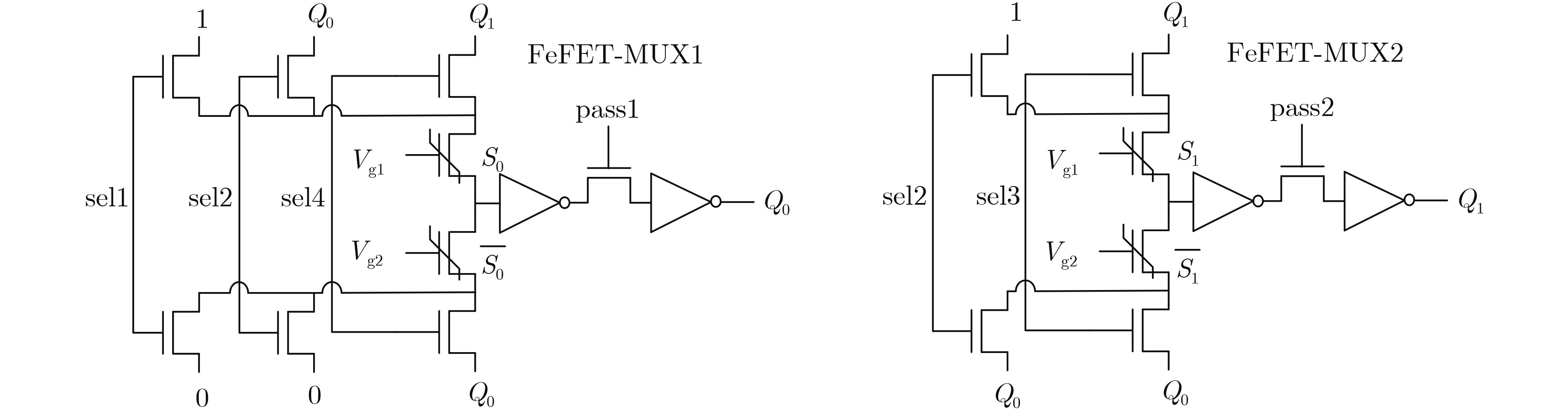
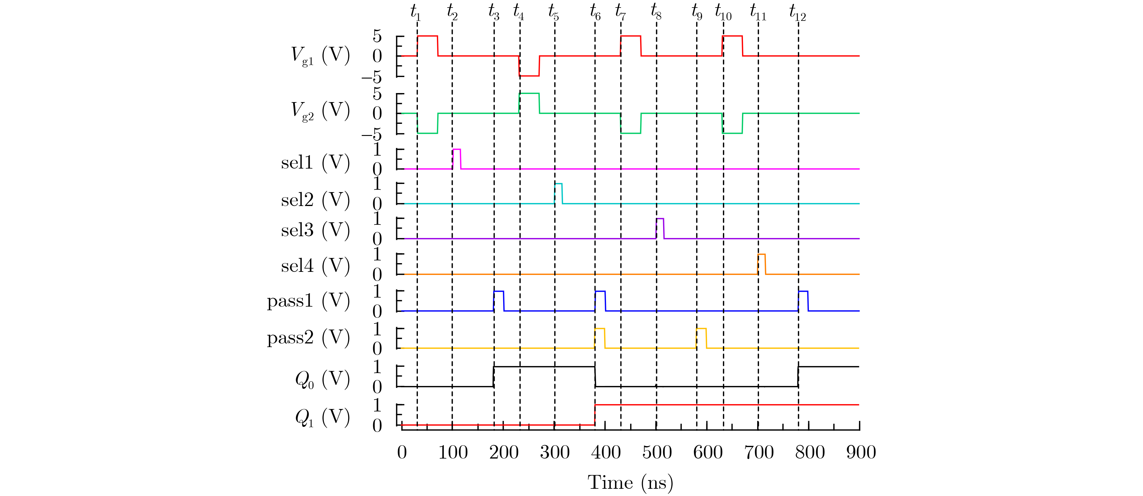
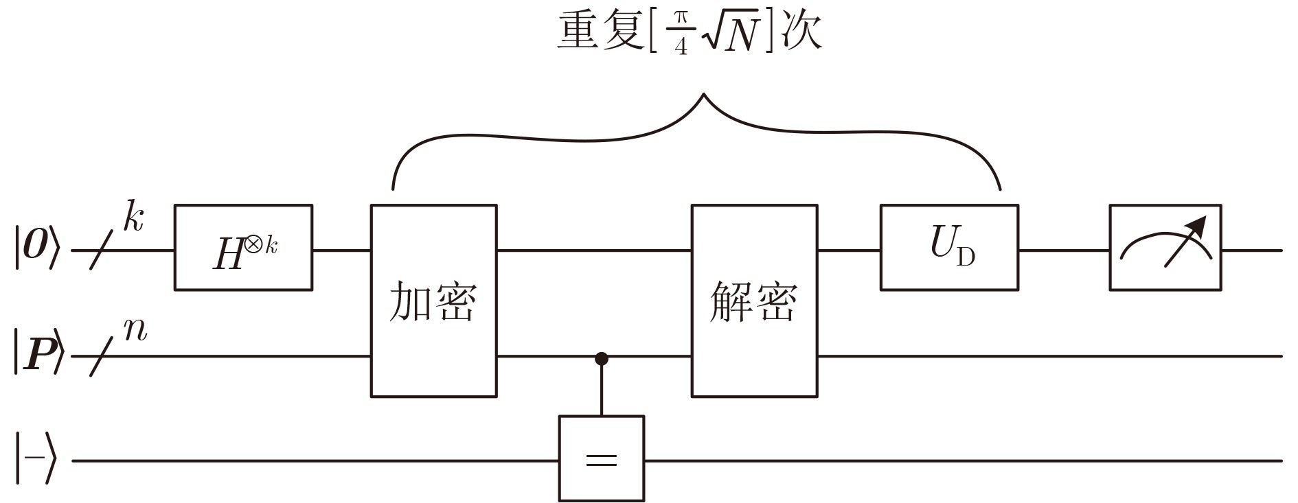
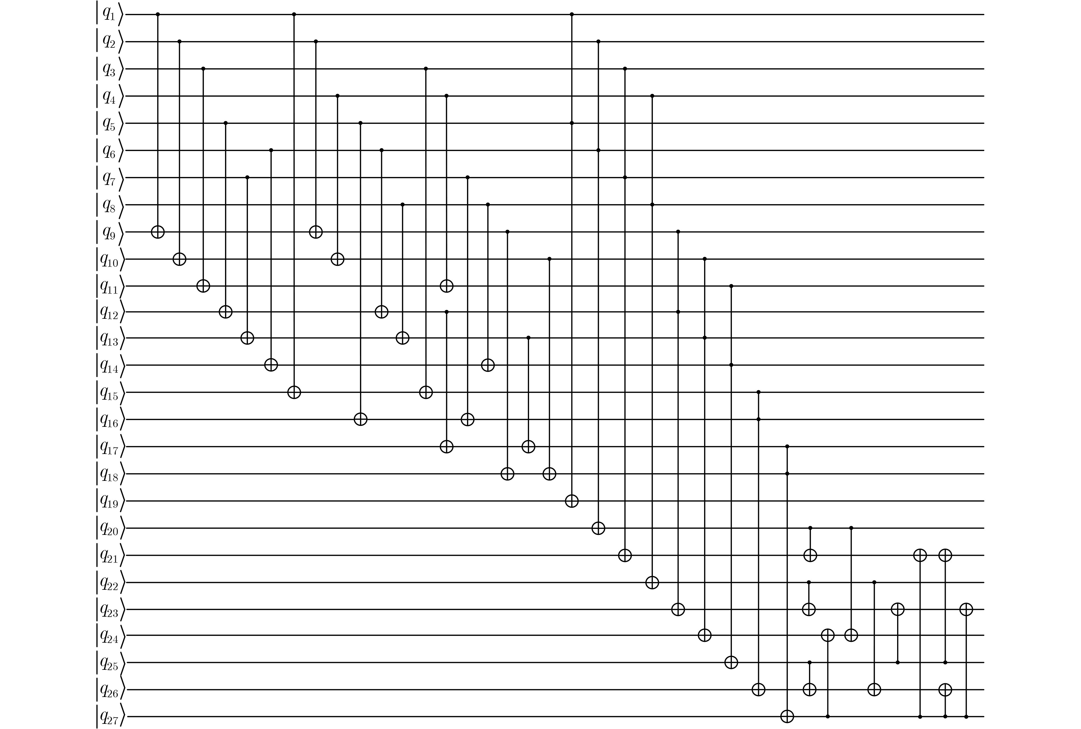
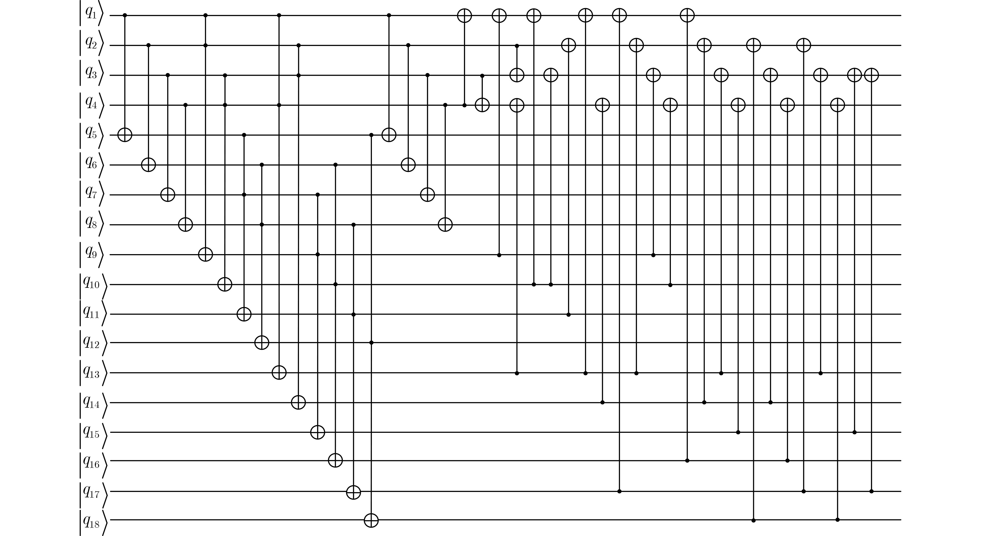
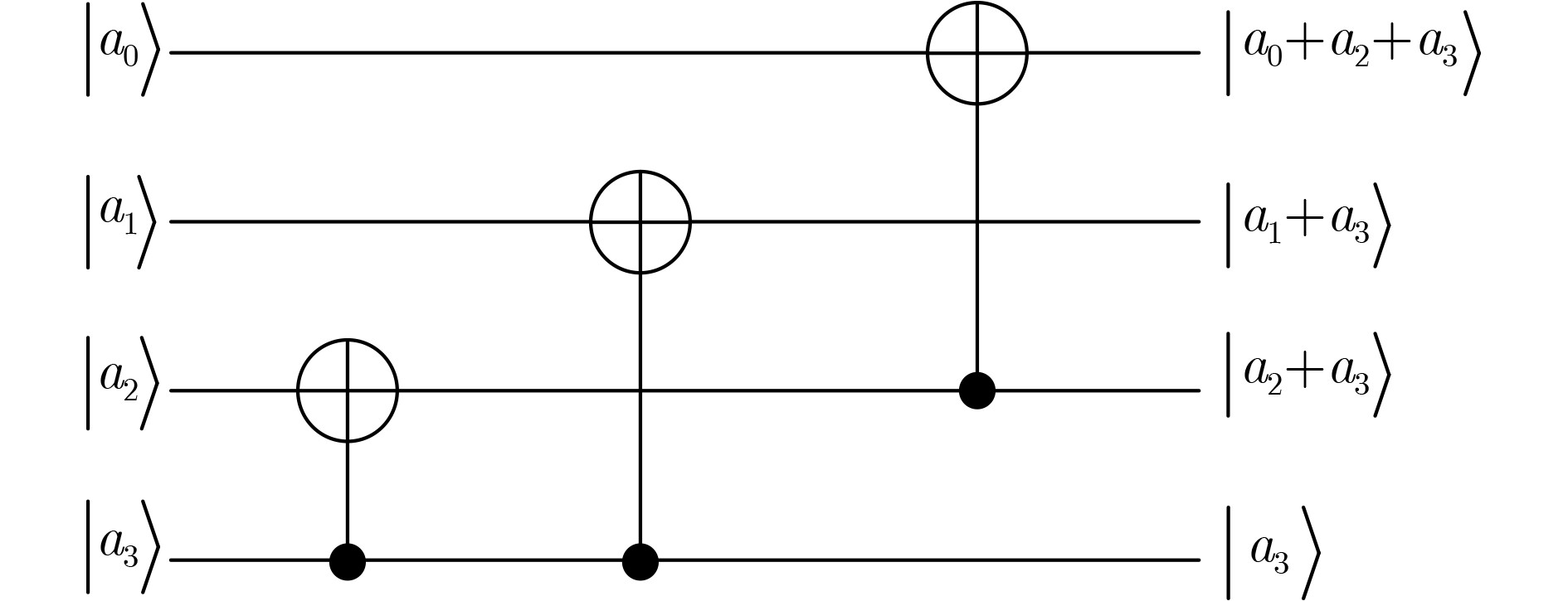
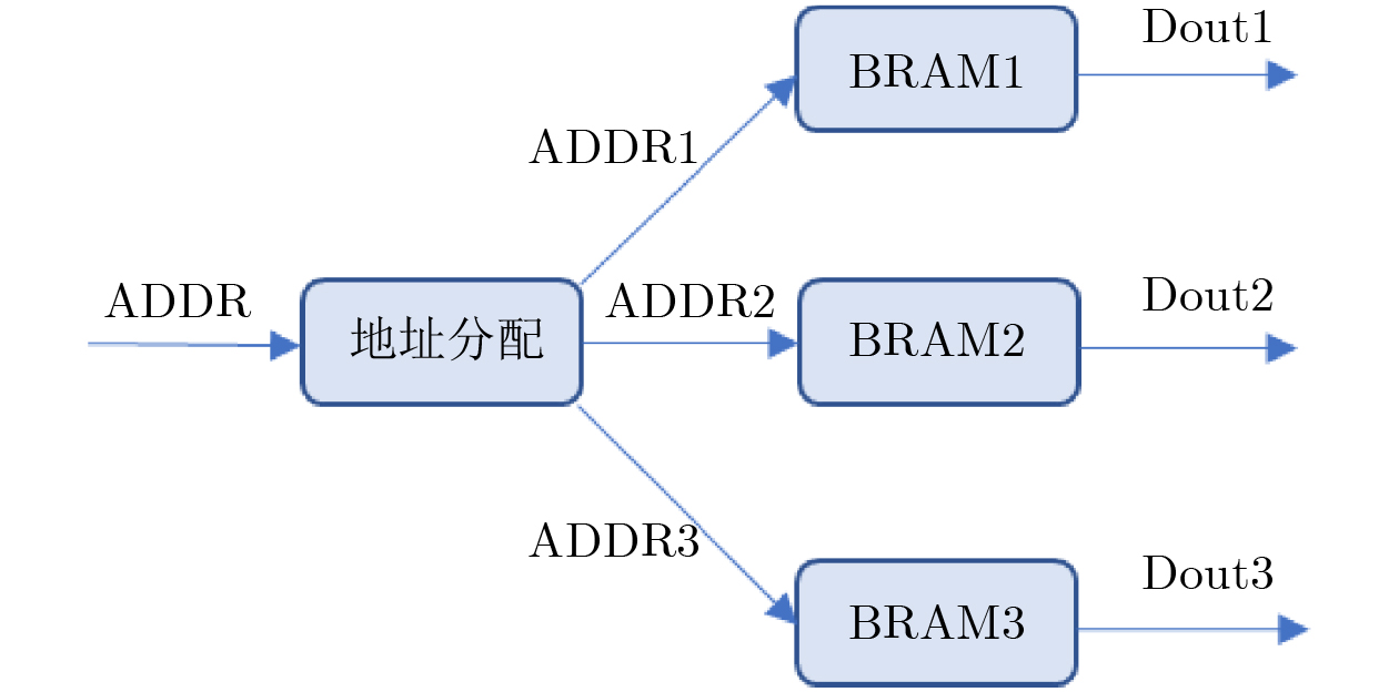
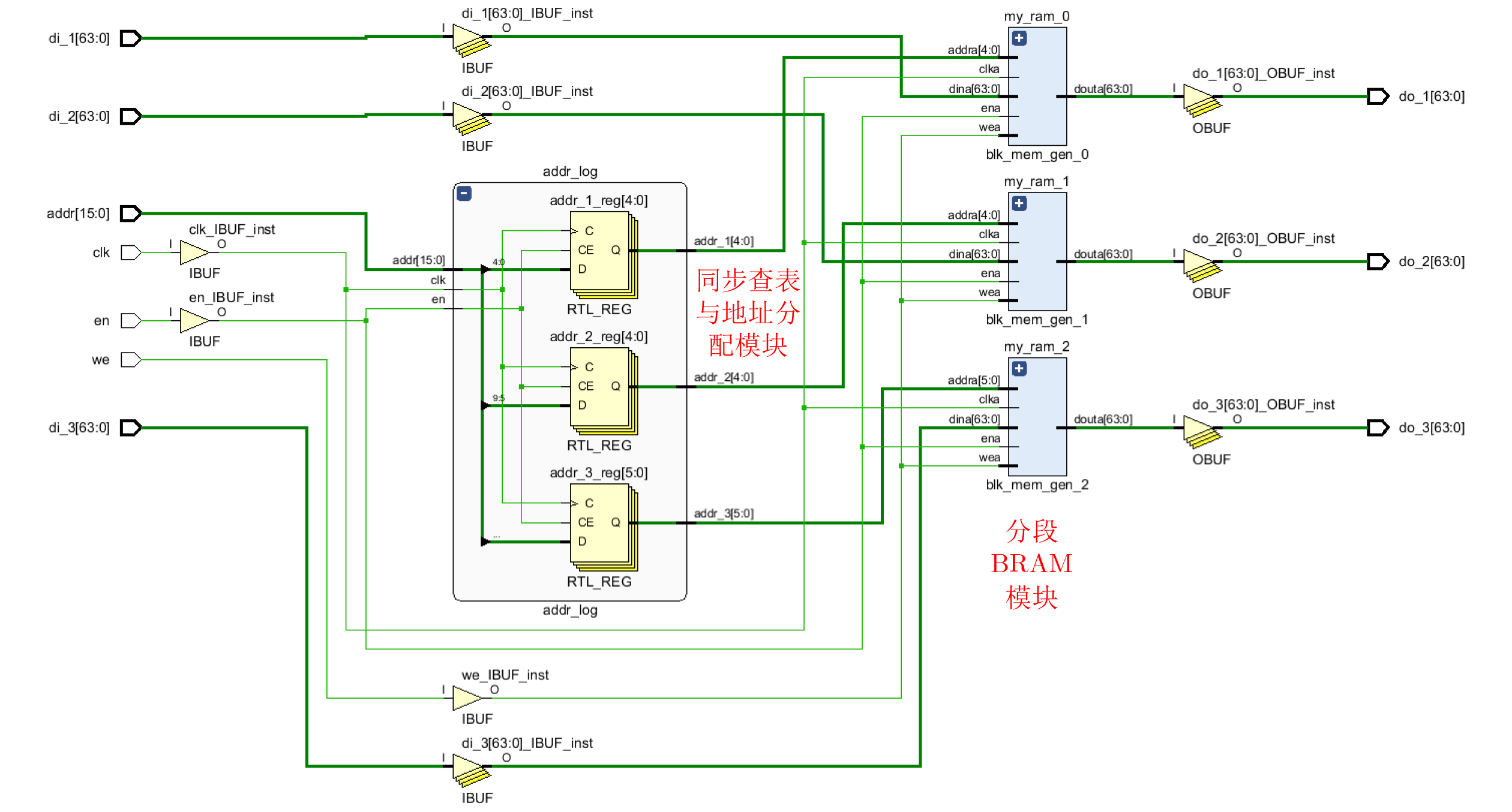
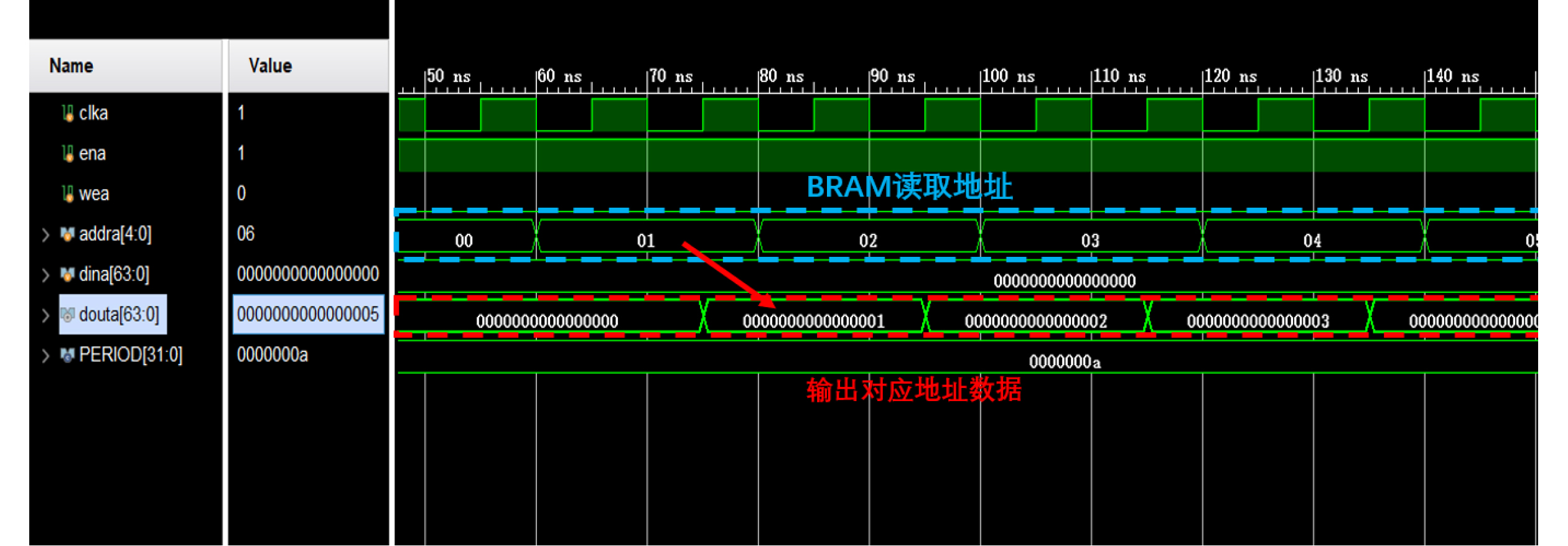
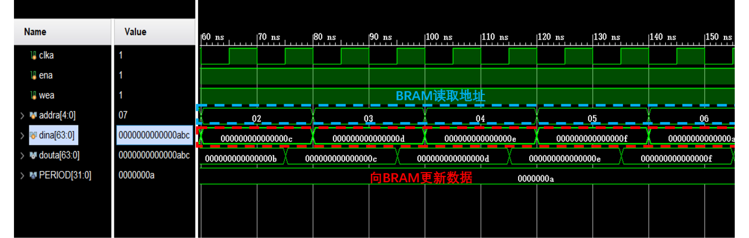
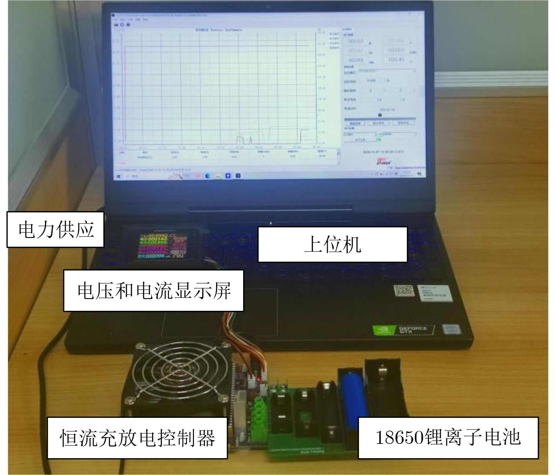
  Significance   Combinatorial Optimization Problems (COPs) are ubiquitous, profoundly impacting diverse fields from logistics and finance to advanced AI and drug discovery. At their core, these problems demand identifying the absolute best solution from an often unfathomably vast set of possibilities. The vast majority of COPs are classified as NP-hard problems, representing one of the most significant computational challenges in computer science. Traditional digital computers, operating on the von Neumann architecture, face immense difficulties in solving COPs; as problem scales expand, required computational resources, particularly latency, increase exponentially. Given these limitations, there’s an urgent need to explore novel architectures for efficiently solving COPs, a pursuit with both significant theoretical importance and profound practical implications for tackling complex, resource-intensive real-world problems. Addressing these challenges, researchers have actively explored various novel hardware-based combinatorial optimization solutions, often transforming COPs into Ising models or Quadratic Unconstrained Binary Optimization (QUBO) problems for hardware implementation. Broadly, existing approaches fall into two categories: digital Application-Specific Integrated Circuit (ASIC) annealers, which suffer from data movement bottlenecks, and dynamical system solvers, which leverage physical dynamics but often demand high device parameter precision, struggle with cross-chip scalability, and may find it difficult to integrate Ising model self-interaction terms. Beyond these, other non-traditional methods like quantum computing (e.g., D-Wave’s quantum annealers requiring cryogenic cooling and having limited connectivity) and certain optical computing approaches (e.g., relying on extremely long optical fibers) exist. While offering unique physical advantages, they generally face substantial challenges in integrating with mature silicon-based Very Large Scale Integration (VLSI) circuits. Consequently, despite a range of novel hardware solutions, their individual limitations highlight the critical need for new combinatorial optimization solvers that offer higher integration, better scalability, superior energy efficiency, and broader problem type support.  Progress   Ferroelectric Field-Effect Transistors (FeFETs), with their unique threshold voltage programmability and multi-port input structure, are opening exciting new avenues for efficiently solving combinatorial optimization problems (COPs). The FeFET-based compute-in-memory (CiM) architecture is particularly well-suited for these challenges, boasting high energy efficiency, low latency, and the inherent ability to accelerate complex operations like vector-matrix and vector-matrix-vector multiplications. Recent research has seen numerous works proposing FeFET-based CiM COP solvers to tackle a diverse range of problems, including those with equality constraints, inequality constraints, and Nash equilibrium scenarios. The overall solving process for these innovative FeFET-based CiM solutions generally involves four key steps: (1) Problem transformation, where the COP is converted into a hardware-friendly objective function, often by encoding equality constraints, introducing slack variables or penalty methods for inequality constraints, or formulating coupled optimization problems for Nash equilibrium scenarios; (2) Following transformation, the objective function undergoes a crucial compression process. This is specifically achieved by analyzing the simulated annealing algorithm itself, which allows for the partial activation of matrix columns, thus significantly reducing the typical computational complexity associated with fully active matrices. Furthermore, this step involves approximating and merging the exponential function components inherent in the algorithm directly into the matrix representation, thereby optimizing the function for efficient hardware implementation on the CiM array; (3) Leveraging the unique three-port and four-port structures of FeFETs, specialized CiM circuit designs are utilized to achieve high-speed acceleration of the compressed objective function. This allows for the efficient computation of a single iteration or a key part of the objective function often within a single clock cycle, significantly mitigating the von Neumann bottleneck; and (4) Finally, based on the optimized and simplified objective function, combinatorial optimization algorithms, such as simulated annealing, are simplified and applied over multiple cycles. This iterative process, efficiently accelerated by the underlying CiM hardware, aims to achieve high-quality and efficient solutions for the given problem. This structured approach highlights the adaptability and potential of FeFET-based CiM for a broad spectrum of challenging combinatorial optimization tasks.  Conclusions  This paper provides a comprehensive review of FeFET-based CiM solvers for solving COPs, which are prevalent across various domains and demand significant computational resources. It first outlines the device characteristics of FeFET and the fundamental process of solving COPs. The core of the paper focused on recent advancements in FeFET-based CiM solvers tailored for three specific scenarios: equality constraints, inequality constraints, and Nash equilibrium. The discussion highlighted how these architectures leverage the unique properties of FeFET to address the computational intensity of these problems.  Prospects   FeFET-based COP solvers show immense potential. By merging FeFET device strengths with CiM advantages, these solvers offer an efficient path to tackling highly complex optimization challenges, leading to substantial gains in speed and energy efficiency for real-world problems. However, significant challenges remain: (1) FeFET endurance is limited, restricting the number of processable problems. (2) Analog-to-digital converters (ADCs) in FeFET CiM arrays incur large area, power, and latency overheads. (3) Simulated annealing algorithms, when applied to large-scale problems, suffer from slow convergence due to increased iterations. Addressing these will be crucial for the widespread adoption and advancement of FeFET-based CiM solutions.
Design of Low-Power On-Chip Cache for Visual Perception Systems on the Edge
CHEN Mo, ZHANG Jing, WANG Yanrong, NAZHAMAITI Maimaiti, QIAO Fei
2025, 47(9): 3116-3125. doi: 10.11999/JEIT250466
Abstract:
  Objective   The proliferation of Internet of Things (IoT) devices and the growing demand for edge computing have driven increased reliance on edge systems. However, deploying compute-intensive tasks on resource-constrained edge devices significantly raises computational demands and power consumption, thereby placing additional strain on energy-limited terminals. On-chip cache, which temporarily stores frequently accessed data and instructions, plays a crucial role in reducing latency and improving system performance. To address the stringent requirements of edge environments, it is essential to design on-chip caches that offer low power consumption, low manufacturing cost, and stable performance.  Methods   The proposed on-chip cache employs SRAM-based storage cells and a block-based architecture to store intermediate data between neural network layers. The memory capacity is configured as 40.5 kbit, based on the output feature map of the first neural network layer, which generates the largest data volume. This feature map has spatial dimensions of 72×72 with 8 channels. To enable efficient data scheduling during neural network computation, data from each channel is stored in an independent sub-array. Therefore, the buffer consists of 8 sub-arrays, each implemented as a 72×72 SRAM array with dedicated bit-line and word-line drivers. A memory control module is implemented to exploit the progressive reduction in data volume across convolutional layers. During access to the second convolutional layer, only the required sub-arrays are activated. Unused memory blocks are dynamically powered down by the control module to achieve deep power optimization. Performance evaluation is carried out through simulations using TSMC 180 nm CMOS technology. The evaluation includes measurements of access latency under different process corners and temperatures; read/write dynamic power consumption under varying supply voltages, temperatures, and clock frequencies; and a comparative analysis of dynamic power consumption between monolithic and block-based storage architectures.  Results and Discussions   The proposed on-chip cache demonstrates strong performance across key evaluation metrics. First, a comprehensive design summary is provided, detailing supply voltage, memory capacity, and layout area under different process variations (Table 1). Second, dynamic read/write power measurements under varying operating temperatures, supply voltages, and clock frequencies (Tables 24) confirm excellent energy efficiency, satisfying the stringent power-performance requirements of edge visual sensing applications across diverse conditions. Access latency analysis further confirms stable memory read/write behavior under process corner variations and thermal fluctuations (Fig. 8). A comparative evaluation of power consumption between monolithic and partitioned storage architectures (Table 5), together with benchmarking against state-of-the-art designs (Table 6), demonstrates that the proposed cache achieves significantly lower read/write energy consumption at the same process node, while maintaining stable access characteristics at reduced operating voltages. This design adopts a system-level optimization strategy that emphasizes architectural innovation over costly process scaling. When implemented in more advanced technology nodes, the architecture is expected to achieve substantial gains in energy-per-access, minimum operating voltage, and area efficiency.  Conclusions   This paper presents the architecture and circuit-level design of an on-chip cache tailored for edge visual perception systems. By optimizing the cache structure for neural network workloads, the proposed design reduces dynamic power consumption through block-based storage and dynamic memory control, thereby enhancing energy efficiency and extending operational endurance. The approach offers broad applicability for edge-based visual perception devices.
Research on Key Technologies of Side-channel Security Protection for Polynomial Multiplication in ML-KEM/Kyber Algorithm
ZHAO Yiqiang, KONG Jindi, FU Yucheng, ZHANG Qizhi, YE Mao, XIA Xianzhao, SONG Xintong, HE Jiaji
2025, 47(9): 3126-3136. doi: 10.11999/JEIT250292
Abstract:
  Objective  As ML-KEM/Kyber is adopted as a post-quantum key encapsulation mechanism, securing its hardware implementations against Side-Channel Attacks (SCAs) has become critical. Although Kyber offers mathematically proven security, its physical implementations remain susceptible to timing-based side-channel leakage, particularly during Polynomial Point-Wise Multiplication (PWM), a core operation in decryption. Existing countermeasures, such as masking and static hiding, struggle to balance security, resource efficiency, and hardware feasibility. This study proposes a dynamic randomization strategy to disrupt execution timing patterns in PWM, thereby improving side-channel resistance in Kyber hardware designs.  Methods  A randomized pseudo-round hiding technique is developed to obfuscate the timing profile of PWM computations. The approach incorporates two key mechanisms: (1) dynamic insertion of redundant modular operations (e.g., dummy additions and multiplications), and (2) two-level pseudo-random scheduling based on Linear Feedback Shift Registers (LFSRs). These mechanisms randomize the execution order of PWM operations while reusing existing butterfly units to reduce hardware overhead. The design is implemented on a Xilinx Spartan-6 FPGA and evaluated using Correlation Power Analysis (CPA) and Test Vector Leakage Assessment (TVLA).  Results and Discussions  Experimental results demonstrate a substantial improvement in side-channel resistance. In unprotected implementations, attackers could recover Kyber’s long-term secret key using as few as 897 to 1,650 power traces. With the proposed countermeasure applied, no successful key recovery occurred even after 10,000 traces, representing more than a 10-fold increase in the number of traces required for key extraction. TVLA results (Fig. 6) confirm the suppression of leakage, with t-test values maintained near the threshold (|t| < 4.5). The resource overhead remains within acceptable bounds: the area-time product increases by 17.99%, requiring only 157 additional Look-Up Tables (LUTs) and 99 Flip-Flops (FFs) compared with the unprotected design. The proposed architecture outperforms existing masking and hiding schemes (Table 3), delivering stronger security with lower resource consumption.  Conclusions  This work presents an efficient and lightweight countermeasure against timing-based SCAs for Kyber hardware implementations. By dynamically randomizing PWM operations, the design significantly enhances side-channel security while maintaining practical resource usage. Future research will focus on optimizing pseudo-round scheduling to reduce latency, extending protection to Kyber’s Fujisaki–Okamoto (FO) transformation modules, and generalizing the method to other Number-Theoretic Transform (NTT)-based lattice cryptographic algorithms such as Dilithium. These developments support the secure and scalable deployment of post-quantum cryptographic systems.
Design of a Bilinear Pairing Coprocessor Based on RISC-V Instruction Extension
YU Bin, MIN Yuxin, ZHANG Zihao, LIU Zhiwei, HUANG Hai
2025, 47(9): 3137-3145. doi: 10.11999/JEIT250367
Abstract:
  Objective  Bilinear pairing operations are fundamental to modern cryptography, forming the basis of advanced systems applied in identity authentication, key exchange, digital signatures, and attribute-based encryption. However, hardware implementations of bilinear pairings face two major challenges: their high computational complexity results in considerable hardware resource consumption, and traditional Field-Programmable Gate Array (FPGA)-based approaches provide limited flexibility. To address these limitations, this study proposes a solution that integrates the RISC-V architecture with Identity-Based Cryptography (IBC) algorithms through instruction set extension and hardwar-software co-design. The proposed approach reduces hardware resource requirements, enhances system flexibility, and enables efficient implementation of cryptographic algorithms.  Methods  The methodology is composed of three main steps. First, conventional state machine-based control logic is replaced by an extended RISC-V instruction set. Six custom instructions are introduced to control arithmetic units for fundamental operations, which transforms the hardware implementation of bilinear pairings from control-intensive to data-intensive circuits, thereby improving hardware resource utilization. Second, to mitigate the bottleneck caused by the bus width limitation of RISC-V, a modular multiplication unit and a bus-efficient modular multiplication mode are designed. By adjusting algorithmic timesteps and employing a small number of on-chip temporary registers, this mode integrates data transmission with computation, allowing transmission and computation cycles to overlap. As a result, the proportion of computation cycles in the overall cycle count is increased, improving system efficiency. Third, a hardware-software co-design strategy is adopted, in which higher-level algorithmic flows are scheduled in software to invoke hardware instructions, thus enhancing system flexibility.  Results and Discussions  (1) Compared with conventional data-intensive circuits, the proposed modular multiplication mode (Fig. 5) effectively reduces the proportion of data transmission cycles in extension field operations. Furthermore, timing optimization of modular multiplication in the quartic extension field (Fig. 6) and the quadratic extension field (Fig. 7) further reduces transmission cycles, thereby improving overall system performance. (2) Relative to FPGA-based implementations of bilinear pairing, the proposed design achieves superior performance in modular multiplication within both the prime field and the quadratic extension field (Table 3). It also shows a clear advantage in terms of Area-Time Product (ATP) for complete bilinear pairing operations. In addition, the design supports flexible adjustment of instruction invocation sequences to accommodate the requirements of different IBC algorithms, leading to a marked improvement in system flexibility.  Conclusions  This paper presents an RISC-V coprocessor that supports bilinear pairing operations for IBC algorithms, addressing the limitations of conventional approaches characterized by high hardware resource consumption, low system utilization, and limited flexibility. A method targeting bus transmission bottlenecks is proposed, which effectively reduces transmission cycle ratios in modular multiplication for quadratic and quartic extension fields. System flexibility is further enhanced by adjusting instruction scheduling to meet the requirements of different IBC algorithms. Future work will focus on exploring pipelined operation modes for more advanced algorithms, using small temporary register groups to further reduce transmission ratios, and achieving cost-effective optimization in data-intensive circuits with balanced area efficiency and computational performance.
Generating Private Key of RSA Encryption Algorithm Using One Time Programmable On-chip Switched Capacitor Physical Unclonable Functions
LI Dawei, CHEN Tienan, ZHOU Yao, JIANG Xiaoping, WAN Meilin, ZHANG Li, HE Zhangqing
2025, 47(9): 3146-3154. doi: 10.11999/JEIT250382
Abstract:
  Objective  RSA, an asymmetric encryption algorithm, is widely recognized as one of the most secure cryptographic methods. Conventional Rivest-Shamir-Adleman(RSA) private keys face challenges of high storage overhead, power consumption, and vulnerability to attacks. To address the dependency on Non-Volatile Memory (NVM) and the risk of physical probing, a novel RSA private key generation architecture is proposed. The design utilizes fully customized Switched Capacitor Physical Unclonable Functions(SC-PUF) cells for random key generation. By mapping the initial output codes of the weak Physical Unclonable Functions(PUF) to the final private key using One-Time Programmable (OTP) memory, the circuit eliminates the need for independent NVM such as flash or EEPROM. This reduces power and area consumption as well as factory testing costs. An integrated capacitive metal shielding layer in the SC-PUF prevents OTP state compromise, thereby ensuring secure key generation.  Methods  The proposed OTP mapping-based scheme is implemented and validated in a security ASIC. A low-cost capacitive SC-PUF circuit is employed to generate stable initial PUF keys through capacitance ratio mismatch sampling, with comprehensive shielding applied to protect the entire PUF and OTP circuitry from invasive attacks. To further mitigate such attacks, Metal-Insulator-Metal (MIM) capacitors constructed from two high-layer metals are used to realize the sense capacitor of the SC-PUF. Both the PUF and OTP circuits are encapsulated within a capacitive-sensitive protective layer. An on-chip CMOS-compatible eFuse-based OTP serves as the mapping circuit, and the OTP, PUF extraction circuit, and mapping circuit are placed beneath the capacitive metal coating provided by the PUF. This architecture enables secure, low-cost, and power-efficient private key generation.  Results and Discussions   The defensive efficacy of SC-PUF and metal shielding against invasive attacks is evaluated by removing the corresponding top metal layer using Focused Ion Beam (FIB) techniques. Although the state of the poly eFuse is directly exposed, complete removal of the top metal layer alters the output key of the SC-PUF (Fig. 7a, b). In a potential attack scenario, all SC-PUF keys may be probed first, followed by metal layer removal to reveal the eFuse state, with the aim of reconstructing the original PUF output codes and mapping control signals. To assess the protective capability of the proposed architecture against such attacks, probing experiments are conducted on the metal layer to determine whether SC-PUF keys can be externally extracted. A total of eight key units are probed (Fig. 7cf). The results show that single-ended probing of the top metal layer leads to a rapid increase in parasitic capacitance to ground, which consistently forces the corresponding output code to 0 (Fig. 7c, e). In contrast, differential probing introduces parasitic capacitance mismatch larger than the original MIM capacitor mismatch, resulting in deviation of the probed output codes from the original values (Fig. 7d, f). Among the eight SC-PUF units tested, five exhibit probe results that differ from the original output codes. These observations indicate that probing the metal layer changes the keys due to parasitic capacitance variations, and the extracted information does not represent the true SC-PUF outputs. Therefore, even if the eFuse state is exposed, the SC-PUF keys cannot be reconstructed and the RSA private key cannot be derived. Additionally, existing implementations generally rely on on-chip NVM to store private keys, making them susceptible to data bus-based probing attacks (Table 1). In contrast, the proposed scheme employs OTP to map the initial weak PUF output codes to the final private key, thereby eliminating the need for independent NVM (Table 1). Although the RSA-2048 algorithm increases logic complexity, leading to a higher gate count and a slight reduction in speed, the proposed OTP mapping-based private key generation circuit achieves a throughput of 187.09 kbps at a power consumption of 218 mW, corresponding to an energy efficiency of 0.858 kbps/mW (Table 1).  Conclusions   To address the dependency on NVM storage and the vulnerability of RSA private keys to physical probing, a novel OTP mapping-based private key generation scheme is proposed. The scheme is programmed at the wafer testing stage, directly mapping the raw PUF output to the target RSA private key, thereby reducing circuit overhead and enabling real-time key generation. This approach effectively mitigates the risk of key interception. Experimental results confirm two key advantages: (1) by mapping the initial output codes of the weak PUF to the final private key through OTP, the scheme eliminates the need for NVM, lowers power and area consumption, and reduces factory test cost. The prototype, fabricated in SMIC 180 nm CMOS technology, occupies 18.77 mm2 and consumes 218 mW; (2) the integrated SC-PUF and metal shielding layer provide effective protection against invasive attacks. This work represents the first application of PUF to RSA private key generation. Furthermore, the proposed scheme can be extended to other asymmetric encryption algorithms requiring private keys, including SM4 and ECC.
A Joint Fault and Congestion-Aware Adaptive Routing Algorithm for Chiplet Interconnect Networks
ZHOU Wu, NI Tianming, XU Dongyu, XU Sheng, LUO Le, CHEN Fulong
2025, 47(9): 3155-3166. doi: 10.11999/JEIT250294
Abstract:
As a key approach to enhancing computing performance and enabling heterogeneous integration in the post-Moore era, chiplet technology relies heavily on the efficiency and reliability of its internal interconnection networks. However, these networks face severe challenges, as frequent link failures and dynamic congestion often coexist and interact, making it difficult to meet the requirements of high-performance and high-reliability systems. To address this issue, this paper proposes a joint Fault- and Congestion-aware Adaptive Routing Algorithm (FCARA). By sensing link status and congestion levels in real time, the algorithm constructs a joint cost function that integrates fault, congestion, and distance factors to dynamically select the optimal path. Simulation-based evaluations and comparisons with benchmark algorithms show that the proposed method markedly reduces average packet delay and improves network saturation throughput. It demonstrates particularly strong performance and robustness under high fault rates and unbalanced traffic conditions. Hardware synthesis and power analysis based on a 65 nm process confirm that the algorithm achieves favorable trade-offs between performance and cost. These findings indicate that the proposed algorithm offers an effective and practical solution to the concurrent challenges of faults and congestion in chiplet interconnect networks.  Objective  With the rapid advancement of chiplet technology as a key solution for post-Moore era computing, the performance and reliability of its internal interconnect network (NoC) have become critical determinants of overall system efficiency. However, chiplet NoCs face unique challenges arising from the concurrent occurrence and coupling of frequent link faults, caused by advanced packaging and high-density interconnects, and dynamic network congestion. Existing routing algorithms typically address these issues in isolation: fault-tolerant methods often overlook the performance degradation introduced by detours under congestion, whereas congestion-aware methods generally assume fault-free networks and fail to adapt when faults occur. These limitations hinder the realization of truly high-performance and highly reliable chiplet systems. Therefore, developing an adaptive routing algorithm that simultaneously and effectively addresses both link faults and network congestion in chiplet interconnects is a crucial requirement.  Methods  To address the challenge, a joint FCARA is proposed for chiplet NoCs. The method is based on real-time, distributed perception of the network state at each router. Information on the fault status of local outgoing links (e.g., normal, partial fault, complete fault) and the congestion level of the input port at the next-hop router is collected. A joint cost function is then employed to quantitatively evaluate potential next-hop directions by integrating three weighted factors: severity of link fault, degree of downstream congestion, and distance to the destination. Using the calculated costs for all available deadlock-free paths, the optimal path with the lowest cost is dynamically selected for forwarding incoming flits. The effectiveness of FCARA is evaluated through extensive cycle-accurate simulations on the ChipletSimulator platform. Performance is compared with baseline algorithms including Dimension-Order Routing (DOR), a representative Fault-tolerant Adaptive Algorithm (FT-Adap), and a representative Congestion-aware Adaptive Algorithm (CA-Adap). Hardware overhead is further assessed through RTL modeling and synthesis using a commercial 65 nm standard cell library, and power consumption is analyzed with Synopsys tools.  Results and Discussions  Simulation results demonstrate the clear advantages of the proposed FCARA algorithm. Across a wide range of fault rates (0%~30%) and traffic patterns, FCARA consistently outperforms baseline algorithms in key performance metrics. In particular, it achieves markedly lower average packet latency and higher network saturation throughput (Fig. 6, Fig. 7). The performance gap becomes especially pronounced under harsh conditions such as high fault rates (≥20%) and non-uniform traffic loads (Fig. 9), highlighting FCARA’s robustness. This improvement results from its joint cost function and adaptive decision-making, which enable it to simultaneously bypass faulty links and congested regions (Algorithm 1). Hardware overhead analysis, based on synthesis and power estimation (Table 2, Table 3), shows that FCARA increases router area by 13.1% and total power consumption by 15.6% compared with the baseline DOR router.  Conclusions  This study developed and evaluated FCARA, a novel adaptive routing strategy tailored for chiplet interconnect networks operating under concurrent link faults and network congestion. The results demonstrate that by jointly incorporating fault and congestion information into routing decisions, FCARA substantially improves network performance in terms of latency and throughput while enhancing robustness compared with conventional approaches that address these issues separately. With its proven effectiveness and moderate hardware overhead, FCARA offers a practical and efficient solution for achieving high-performance, high-reliability communication in next-generation chiplet-based systems.
Optimizing Output Obfuscation of Logic Locking with Linear Programming
QIN Weirong, CUI Xiaotong, CHENG Kefei
2025, 47(9): 3167-3177. doi: 10.11999/JEIT250527
Abstract:
  Objective  The globalization of the Integrated Circuit (IC) supply chain has created a crisis of hardware trust, exposing systems to hardware security threats. Logic locking, a key Design-For-Trust (DFT) technique, protects hardware designs by inserting key-driven gates that obfuscate the original circuit, thereby mitigating threats such as intellectual property theft and hardware Trojans. The effectiveness of logic locking is determined by its output obfuscation level, which directly influences resilience against existing attacks. This level is quantified by two sub-metrics: randomness and inconsistency. Weakness in either sub-metric enables targeted attacks, and current methods achieve limited performance on both, restricting their practical security guarantees. To address these limitations, this study proposes a logic locking approach that improves the output obfuscation level of locked circuits using linear programming.  Methods  A Linear Programming-based Logic Locking (LPLL) method is proposed to optimize output obfuscation under incorrect keys. The core idea is to model each circuit gate as a set of linear constraints, thereby transforming the objective of maximizing the output obfuscation level into a solvable linear objective function. This formulation determines the optimal placement of key gates that are specifically activated by incorrect keys. Because adversaries in real-world attack scenarios rely on random key guessing, key gates may remain inactive, leading to weakened obfuscation. To address this vulnerability, an auto-incrementing key selection algorithm is introduced. This algorithm iteratively builds upon and inherits prior optimization results, thereby strengthening robustness. The iterative mechanism ensures persistent output corruption: even if key gates selected at later stages remain inactive, obfuscation is still enforced by those optimized in earlier iterations.  Results and Discussions  Experimental results demonstrate that the proposed LPLL method substantially enhances output obfuscation. For equivalent key sizes, LPLL markedly increases the randomness of output obfuscation, consistently sustaining a high degree of unpredictability. Quantitatively, it improves the probability of randomness by up to 24.1% compared with Fault analysis-based Logic Locking (FLL) and by 49.9% compared with Random Logic Locking (RLL) (Fig. 4). In addition to randomness, LPLL exhibits a clear advantage in output obfuscation inconsistency. While both LPLL and FLL achieve improved inconsistency with increasing key sizes, LPLL consistently reaches higher inconsistency values across most scenarios. Specifically, it raises the probability of inconsistency by up to 24.1% relative to FLL and by 62.5% relative to RLL (Fig. 5). This advantage is particularly pronounced at smaller key sizes, where LPLL achieves greater inconsistency spread and more efficient key utilization, making it especially suitable for resource-constrained applications.  Conclusions  This work presents LPLL, an approach that redefines logic locking by mapping complex circuit structures onto a linear programming model. The method systematically formulates optimal key-gate selection as a solvable linear optimization problem. To further strengthen security, LPLL incorporates an auto-incrementing key selection algorithm that establishes an iterative mechanism, ensuring persistent high-level output obfuscation even under dynamic attack conditions. LPLL not only exceeds existing methods such as RLL and FLL)in output obfuscation metrics but also, more importantly, provides a systematic and quantifiable paradigm for determining key-gate layouts. This research offers a forward-looking perspective for the design of trustworthy hardware.
Mitigating Cache Side-channel Attacks via Fast Flushing Mechanism
ZHENG Shuai, XU Xiangrong, XIAO Limin, LIU Hao, XIE Xilong, YANG Rui, RUAN Li, LIAO Xiaojian, LIU Shanfeng, ZHANG Wancai, WANG Liang
2025, 47(9): 3178-3186. doi: 10.11999/JEIT250471
Abstract:
  Objective  With the rising demand for secure computing, cache-based side-channel attacks have become a critical threat to modern processors. Conventional data cache designs do not account for information leakage caused by malicious memory access patterns, enabling adversaries to infer sensitive data from subtle variations in cache access latency. Existing countermeasures, such as cache mapping randomization and cache flushing, provide partial protection but incur considerable hardware overhead and performance degradation, particularly in resource-constrained private caches such as L1 and L2. To address this limitation, this study focuses on L1 data caches and proposes a fast flushing mechanism based on Time-To-Live (TTL) control. The method mitigates side-channel leakage while minimizing additional hardware complexity and performance cost.  Methods  This study proposes a fast cache flushing method that introduces a lightweight 3-bit TTL field into each cache line, together with a global time register (Time), to enable efficient cache invalidation. When a flush instruction is issued, the Time register is incremented, and all cache lines are checked against their TTL values. Only lines that remain valid and contain modified data are invalidated and written back, thereby reducing flushing overhead. To ensure robustness and correctness, several auxiliary strategies are incorporated, including mechanisms to handle TTL wraparound, preserve data consistency, and strengthen resistance against advanced side-channel attacks. The proposed mechanism is realized through custom instruction set extensions on an RISC-V processor platform.  Results and Discussions  The proposed cache flushing mechanism exhibits significant performance benefits in representative application scenarios. Experimental evaluation shows that it reduces average flushing latency by approximately 70% relative to conventional flushing techniques. In side-channel security tests based on the Prime+Probe attack model, an adversary probing 1024 cache lines after the victim executes a flush operation is unable to recover valid sensitive information patterns, thereby confirming the security effectiveness of the proposed architecture. Regarding hardware overhead, the design introduces only about 8% additional logic and approximately 0.01% extra storage cost for TTL fields compared with conventional cache structures.  Conclusions  This paper presents a fast cache flushing mechanism to defend against cache-based side-channel attacks. The proposed method achieves a balanced trade-off between security and performance. Experimental results show that it substantially reduces cache flushing latency while effectively mitigating typical side-channel threats. The design is particularly suited for deployment in resource-constrained private caches such as L1 and L2. Hardware implementation further confirms the lightweight nature and engineering feasibility of the approach, indicating strong potential for practical application.
Collaborative Optimization Strategies for Matrix Multiplication-Accumulation Operators on Commercial Processing-In-Memory Architectures
HE Yukai, XIE Tongxin, ZHU Zhenhua, GAO Lan, LI Bing
2025, 47(9): 3187-3197. doi: 10.11999/JEIT250364
Abstract:
  Objective  Processing-In-Memory (PIM) architectures have emerged as a promising solution to the memory wall problem in modern computing systems by bringing computation closer to data storage. By minimizing data movement between processor and memory, PIM reduces data transfer latency and energy consumption, making it well suited for data-intensive applications such as deep neural network inference and training. Among various PIM implementations, Samsung’s High Bandwidth Memory Processing-In-Memory (HBM-PIM) platform integrates simple computing units within HBM devices, leveraging high internal bandwidth and massive parallelism. This architecture shows strong potential to accelerate compute- and memory-bound AI operators. However, our observations reveal that the acceleration ratio of HBM-PIM fluctuates considerably with matrix size, resulting in limited scalability for large model deployment and inefficient utilization for small- and medium-scale workloads. Addressing these fluctuations is essential to fully exploit the potential of HBM-PIM for scalable AI operator acceleration. This work systematically investigates the causes of performance divergence across matrix scales and proposes an integrated optimization framework that improves both scalability and adaptability in heterogeneous workload environments.  Methods  Comprehensive performance profiling is conducted on matrix-vector multiplication GEneral Matrix Vector Multiplication (GEMV) operators executed on an HBM-PIM simulation platform (Fig. 2, Fig. 3), covering matrix sizes from 1 024 × 1 024 to 4 096 × 4 096. Profiling results (Table 1, Table 2) indicate that at smaller matrix scales, hardware resources such as DRAM banks are underutilized, leading to reduced bank-level parallelism and inefficient execution cycles. To address these bottlenecks, a collaborative optimization framework is proposed, consisting of three complementary strategies. First, a Dynamic Bank Allocation Strategy (DBAS) is employed to configure the number of active banks according to input matrix dimensions, ensuring alignment of computational resources with task granularity and preventing unnecessary activation of idle banks. Second, an Odd-Even Bank Interleaved Address Mapping (OEBIM) mechanism is applied to distribute data blocks evenly across active banks, thereby reducing access hotspots and enhancing memory-level parallelism. Third, a Virtual Tile Execution Framework is implemented to logically aggregate multiple fine-grained operations into coarser-grained execution units, effectively reducing the frequency of barrier synchronization and host-side instruction dispatches (Algorithm 1, Fig. 5, Fig. 6). Each strategy is implemented and evaluated under controlled conditions using a cycle-accurate HBM-PIM simulator (Table 3). Integration is performed while maintaining compatibility with existing hardware configuration constraints, including the 8-lane register file limits per DRAM bank.  Results and Discussions  Experimental results (Fig. 7) show that the optimization framework delivers consistent and substantial performance improvements across different matrix scales. For instance, with a 2 048 × 2 048 matrix input, the acceleration ratio increased from 1.296 (baseline) to 3.479 after optimization. With a 4 096 × 4 096 matrix, it improved from 2.741 (baseline) to 8.225. Across all tested sizes, the optimized implementation achieved an average performance gain of approximately 2.7× relative to the baseline HBM-PIM configuration. Beyond raw acceleration, the framework improved execution stability by preventing the performance degradation observed in baseline implementations under smaller matrices. These results demonstrate that the combination of dynamic resource allocation, balanced address mapping, and logical operation aggregation effectively mitigates resource underutilization and scheduling inefficiencies inherent to HBM-PIM architectures. Further analysis confirms that the framework enhances scalability and adaptability without requiring substantial hardware modifications. By aligning resource activation granularity with workload size and reducing host-device communication overhead, the framework achieves better utilization of available parallelism at both memory and computation levels. This leads to more predictable performance scaling under heterogeneous workloads and strengthens the feasibility of deploying AI operators on commercial PIM systems.  Conclusions  This study presents a collaborative optimization framework to address performance instability of GEMV operators on commercial HBM-PIM architectures under varying matrix scales. By combining dynamic bank allocation, odd-even interleaved address mapping, and virtual tile execution strategies, the framework achieves consistent and scalable acceleration across small to large matrices while enhancing execution stability and resource utilization. These findings provide practical guidance for software-hardware co-optimization in PIM-based AI acceleration platforms and serve as a reference for the design of future AI accelerators targeting data-intensive tasks. Future work will focus on extending the framework to additional AI operators, validating its effectiveness on real hardware prototypes, and investigating integration with compiler toolchains for automated operator mapping and scheduling.
A Probability-Based Parasitic Extraction Algorithm for Global-Routed VLSI Designs
CHEN Jiarui, WU Zhaoyi, YOU Yongjie, CHEN Yilu, LIN Zhifeng
2025, 47(9): 3198-3207. doi: 10.11999/JEIT250458
Abstract:
  Objective  Parasitic extraction is a critical stage in the VLSI design flow, as it determines the parasitic parameters of interconnect wires, directly affecting delay evaluation, timing analysis, and performance verification. With the increasing complexity of modern designs, accurate estimation of parasitic parameters has become a central challenge in routing. Developing a fast and accurate extraction algorithm is therefore essential to enable high-performance routing solutions.  Methods  Pattern matching is a widely used technique for full-layout parasitic extraction. Given an interconnect layout, the method divides it into small sections and determines the parasitics of each section with a pre-built pattern library. However, with billions of transistors placed on a single chip, the continuous growth of design complexity makes full-layout parasitic extraction increasingly challenging. Inspired by pattern matching, this paper presents a probability-based parasitic extraction algorithm tailored for modern VLSI designs. The proposed method consists of two main stages: (1) layout analysis and (2) parasitic extraction. Given a global-routed netlist and technology files containing pre-characterized parasitic values, layout analysis captures coupling segment information and generates a probability-based look-up table for efficient wire-spacing computation. Parasitic extraction then constructs the RC tree for each net and produces accurate interconnect parasitic parameters using the spacing information derived from layout analysis. For layout analysis, a partitioning strategy is employed to identify coupling segments that are parallel to and overlap with the target wire segment. In practice, coupling segments far from the target wire exert negligible effects on parasitics; therefore, the chip layout is divided into regions to improve identification efficiency. During parasitic extraction, coupling segments in both the same layer and in abutting layers are considered. If the target wire fully traverses the grids in an adjacent layer, all segments in those grids are treated as cross segments; otherwise, only partially overlapping segments are included. Once the coupling segments are determined, wire spacing must be calculated. In parasitic extraction, spacing represents the distance between a wire and its nearest neighbor. Because of the vast number of wires in modern circuits, computing exact spacing for every wire is prohibitively expensive. To address this, a probability-based average spacing model is proposed. In multilayer circuit designs, extraction also requires accurate reconstruction of routing information from layout data. In the standard Design Exchange Format (DEF), routing topology is represented by wires and vias. To handle this efficiently, a construction algorithm is developed to build connected RC trees from distributed wires and vias. Leveraging the probability-based wire-spacing model together with the technology files, the algorithm extracts parasitic parameters while accounting for coupling effects. The technology file “.captbl” provides interconnect parasitic tables indexed by wire width and spacing, with widths varying across different metal layers due to process constraints. Interpolation methods are first applied to obtain the unit resistance as a function of wire spacing and width. Wire resistance is then modeled by multiplying this unit resistance by wire length. Similarly, capacitance is extracted using interpolation, with additional coupling effects between neighboring layers captured through a grid-based recognition strategy that identifies the number of cross segments. Relative coupling capacitance is then determined accordingly.  Results and Discussions  Experiments were conducted on twelve industrial designs to evaluate the proposed extraction algorithm. The results demonstrate that the method achieves high parasitic accuracy while being 21.6% faster than the commercial tool Innovus. The average capacitance error is 1.15% with a standard deviation of 3.09%, and the average resistance error is 0.08% with a standard deviation of 2.63%. Notably, for all twelve circuits, the standard deviation of both capacitance and resistance errors remains below 5%. These findings confirm that the proposed algorithm provides both accuracy and efficiency for full-chip parasitic extraction, offering a practical foundation for developing high-performance routing algorithms.  Conclusions  This paper presents a probability-based parasitic extractor for addressing full-chip extraction challenges. A partitioning strategy with grid-based data representation is developed to capture coupling segments efficiently. Based on these segments, a probability-driven mathematical model is proposed to calculate wire spacing, with a pre-computed look-up table accelerating the computation. An efficient construction algorithm is further presented to build connected RC trees from distributed wires and vias, followed by a coupling-aware RC extraction method to produce accurate interconnect parasitics. Experimental evaluation on twelve industrial benchmarks demonstrates strong correlation between the extracted parasitics and those obtained from the commercial tool Innovus.
Design of Efficient ORBGRAND Decoders with Parity-Check Constraint
LEI Sheng, LIANG Zhanhua, TIAN Jing, ZHOU Yangcan
2025, 47(9): 3208-3219. doi: 10.11999/JEIT250501
Abstract:
  Objective  Ordered Reliability Bits Guessing Random Additive Noise Decoding (ORBGRAND) is a universal channel decoding algorithm characterized by its simple principles, strong decoding performance, low average latency, and hardware-friendly implementation. Since its proposal, ORBGRAND has attracted considerable attention as a promising alternative to traditional decoding methods. By combining ordered reliability bits with a noise-guessing strategy, it achieves near Maximum-Likelihood Decoding (MLD) performance while avoiding prohibitive resource overhead. However, challenges remain: its worst-case latency and limited throughput restrict practical use in high-speed communication systems. To address these gaps, this work proposes improved ORBGRAND serial and unrolled hardware architectures that incorporate a special parity-check constraint.  Methods  This study proposes incorporating a specific parity-check constraint into serial and unrolled ORBGRAND architectures. In the serial architecture, the global parity-check bit is used to control the iteration of Hamming Weight (HW) and Logistic Weight (LW), enabling the decoder to skip the generation and verification of invalid error patterns. In the unrolled architecture, error patterns are separately pre-stored and queried according to the global parity-check bit. This design significantly enhances the hardware efficiency of ORBGRAND decoders.  Results and Discussions  The improved serial and unrolled ORBGRAND decoders with the global parity-check constraint are implemented and compared with their original counterparts. Simulation results for a tested code indicate that the parity-check constraint preserves the decoding performance of conventional ORBGRAND, while reducing the average number of error pattern queries by 50% in the low to medium Signal-to-Noise Ratio (SNR) range. The architectures are synthesized using Synopsys Design Compiler with TSMC 28 nm technology. The serial ORBGRAND architecture achieves an operating frequency of 400 MHz, delivering a throughput of 33.1 Gbps at SNR = 8 dB. The implementation occupies 0.18 mm2 of area, yielding an area efficiency of 183.9 Gbps/mm2. Compared with the prior art, the serial design increases throughput by 80.9% and area efficiency by 48.1%. The unrolled architecture achieves a throughput of 110.6 Gbps and an area efficiency of 3.97 Gbps/mm2, corresponding to improvements of 584% in throughput and 1223% in area efficiency relative to the prior art.  Conclusions  The ORBGRAND algorithm offers a promising approach for high-performance decoding in communication systems by combining high parallelism with near MLD performance. The specific parity-check constraint filters out invalid error patterns, significantly reducing the number of error pattern queries in serial and unrolled ORBGRAND architectures, without compromising performance. The serial and unrolled architectural implementations achieve notable gains in throughput and area efficiency compared with original designs. Integrating ORBGRAND with parity-check constraints thus represents a significant advancement, providing a more efficient solution for pratical communication applications. Future work will focus on further optimization of these architectures and their adaptation to diverse communication standards. In particular, the exploration of additional coding contraints may further extend the applicability of the approach.
Research on Optimization Methods for Static Random-Access Memory-Physical Unclonable Function Key Extraction
JIANG Dongmei, TANG Xusheng, LI Bing, ZHANG Qingyu, HE Weiguo
2025, 47(9): 3220-3229. doi: 10.11999/JEIT250551
Abstract:
  Objective  Non-Volatile Memory (NVM) storage keys are exposed to physical attacks, and most lightweight Internet-of-Things (IoT) devices cannot deploy costly protection. A Physical Unclonable Function (PUF) offers a practical defense. However, Static Random-Access Memory PUFs (SRAM-PUFs) used as key generators exhibit environmental sensitivity that degrades stability. Therefore, optimization methods for SRAM-PUF–based key extraction fall into three main categories: (1) circuit-level enhancements that modify the SRAM cell to strengthen its inherent 0/1 bias; (2) cell selection methods that identify and retain only stable cells through dedicated algorithms; and (3) fuzzy-extractor schemes tailored to SRAM-PUFs that correct residual noise to yield reproducible cryptographic keys.  Methods  The selection of SRAM cells can markedly enhance bit stability. However, although reducing the complexity of Error-Correcting Code (ECC) encoding and decoding, this approach requires consuming a large number of stable cells to satisfy key entropy requirements, which in turn increases ECC code length. To address this contradiction, this paper proposes a new key extraction scheme (Figure 2). In the proposed method, SRAM bits are divided into stable and noisy categories. The high entropy of noisy bits is leveraged for key generation: noisy bits are hashed to produce entropy-rich values, whereas stable bits with a low bit error rate are used to generate PUF responses. In the registration stage, the synthesized key is rearranged to form m vectors ( R 1, R 2,···, R m) according to m different rules. These m vectors are then combined into a new vector R . A repetition code of length 2t+1 (able to correct t errors) is applied to R to generate a codeword C . The codeword C is XORed with the PUF response to obtain helper data w, which is stored in NVM. In the reconstruction stage, w is XORed with a new PUF response to obtain C ′. Due to the repetition coding applied during registration, decoding is performed using a majority decision rule with a threshold of t+1. The decoding result R ' is reshaped into a matrix D with m rows and x columns, followed by reverse interleaving based on the rules used in registration. A majority decision is then executed independently for each column, with a decision threshold of m/2+1. The recovered key is output as the final result.  Results and Discussions  SRAM. Tests at –40 °C, 25 °C, and 85 °C show that the proposed bit-selection algorithm reduces the bit-change rate of SRAM-PUFs, with the number of screenings inversely proportional to the average change rate. The bit-change rate is highest at elevated temperatures. After 20 screenings, the average change rate at 85 °C decreases from 0.14 to 0.07, and after 80 screenings, it further decreases to 0.06. A quantitative analysis of error-correction capability is also performed. Based on the measured bit-change rates at high temperatures, the probability of key reconstruction failure is derived as low as 1.487 6E–9. In addition, 1 024 byte of SRAM cells are shown to yield entropy keys of 128 bit.  Conclusions  This paper proposes a novel SRAM-PUF key extraction scheme that resolves the trade-off between stability requirements and high entropy demands by employing a bit-selection algorithm. The scheme simplifies error-correction encoding and decoding while enhancing the entropy of the generated keys. Compared with existing approaches, the computational complexity is reduced by 40% relative to Scheme 2, by 98.9% relative to Scheme 3, and by 99.12% relative to Scheme 4. Furthermore, the method provides an integrated solution for screening stable SRAM cells, highlighting its practical application potential. Based on the bit error rate of 28 nm SRAM-PUFs, the key reconstruction success rate is calculated as (1–1.4876E–9). In tests conducted at –40 °C, 25 °C, and 85 °C, with 200 key reconstruction attempts per condition, all 11 chips achieved successful reconstruction. Considering variations across different fabrication processes, the number of screening cycles as well as parameters m and t can be adjusted to accommodate other process nodes.
High-Performance Hardware Design of Arithmetic Coding for Deep Neural Network-Based Image Compression
SONG Sai, CUI Zhao, ZHAN Yinseng, YANG Jinzhen, LU Ming, TIAN Jing
2025, 47(9): 3230-3240. doi: 10.11999/JEIT250509
Abstract:
  Objective  Deep Neural Network (DNN)-based image compression has gained increasing importance in real-time applications such as intelligent driving, where an efficient balance between compression ratio and encoding speed is essential. This study proposes a hardware implementation of entropy coding, realized on a Field-Programmable Gate Array (FPGA) platform based on Range Asymmetric Numeral Systems (RANS) arithmetic coding. The design seeks to achieve an optimal trade-off between compression efficiency and hardware resource utilization, while maximizing data throughput to meet the requirements of real-time environments. The main objectives are to enhance image encoding throughput, reduce hardware resource consumption, and sustain high data throughput with only minor losses in compression ratio. The proposed hardware architecture demonstrates strong scalability and practical deployment potential, offering significant value for DNN-based image compression in high-performance systems.  Methods  To enable practical FPGA deployment of RANS arithmetic coding, several hardware-oriented optimizations are applied. Division and modulus operations in the state update are replaced with precomputed reciprocals combined with fixed-point multiply-and-shift sequences. A precision-calibration stage based on remainder-boundary checks corrects substitution errors to ensure exact quotient-remainder equivalence with full-precision division. This calibration is implemented synchronously in the encoder datapath with minimal control overhead to preserve lossless decoding. Parameter storage and lookup overheads are reduced through fine-grained quantization and a compact, flattened Cumulative Distribution Function (CDF) layout, CDF values are linearly scaled and quantized to fixed-width integers, while contiguous storage of valid entries together with stored effective lengths eliminated padding. Tailored bit-width assignments for different parameter types balance precision against resource usage. These measures reduce the CDF table size from 31.125 kB to 6.369 kB while simplifying lookup logic and shortening critical memory-access paths. Throughput is further increased by using an interleaved multi-channel architecture in which the input stream is partitioned into independent substreams processed concurrently by separate RANS encoder instances. Each instances maintain its own local state, parameter memory, and renormalization buffer. Local handling of renormalization and escape conditions preserves channel continuity, enabling the decoder to perform symmetric decoding without global synchronization. Finally, the entire design is organized as a pipeline-friendly datapath. Reciprocal multiplications are mapped to DSP blocks, while lookups and calibration checks occupy adjacent pipeline stages. Renormalized bytes are emitted to an output FIFO to avoid stalls. This eliminates multi-cycle divide units, reduces latency and memory footprint, and provide a scalable path to high-frequency, high-throughput operation.  Results and Discussions  The proposed model is deployed on a Xilinx Kintex-7 XC7K325T FPGA platform, synthesized using Vivado v2018.2 and functionally verified on ModelSim SE-64 10.4. Data throughput, resource utilization, and compression efficiency are emphasized in the evaluation. Simulation results indicate that the implemented encoder achieves an identical compression ratio to the PyTorch-based open-source CompressAI library. Any degradation in compression efficiency caused by high parallelism is negligible for high-resolution images (≥768 × 512) (Fig. 5). The FPGA implementation further shows that timing closure is met at a 140 MHz clock frequency. In single-channel mode, the design consumes only 540 LUTs, 336 FFs, and 9.5 BRAMs. Under high-parallelism configurations, resource utilization scales linearly with the number of channels. In eight-channel parallel mode, the encoder attains a symbol throughput of 191.97 MSymbols/s and a data throughput of 4.607 Gbps, representing an improvement of approximately 766% over single-channel operation (Table 3). To quantitatively evaluate the trade-off between resource usage and encoding efficiency, the metric Area Efficiency (AE) is introduced. When compared with FPGA implementations of other entropy coding schemes, the proposed architecture demonstrates clear advantages in both resource efficiency and throughput, achieving an AE of 85.97 kSymbol/(s·Slice), which exceeds most existing high-throughput models. Relative to comparable entropy coding schemes, the proposed design provides a significant increase in throughput (Table 4). Moreover, the scalability and adaptability of the architecture are validated across different degrees of parallelism, enabling flexible adjustment of channel count while maintaining superior performance in diverse application scenarios.  Conclusions  This work proposes a high-throughput RANS arithmetic coding hardware architecture for DNN-based image compression and demonstrates its implementation on an FPGA platform. By integrating hardware-friendly division substitution, fine-grained parameter quantization, and continuous-output interleaved parallelism, the design overcomes key bottlenecks related to computational latency and resource overhead. Experimental results confirm that the proposed model achieves a peak throughput of 191.97 Msymbols/s with negligible compression loss, while also demonstrating outstanding AE and linear scalability. The architecture provides significant advantages over existing entropy coding implementations in both resource-constrained and high-performance scenarios, offering strong practical potential for real-time neural network image compression systems. Overall, this research delivers a pragmatic and extensible solution for the hardware realization of DNN-based image compression, with the capability to accelerate large-scale deployment in high-efficiency environments such as intelligent driving.
Automated Discovery of Exploitable Instruction Patterns for KASLR Circumvention
LI Zhouyang, QIU Pengfei, QING Yu, WANG Chunlu, WANG Dongsheng
2025, 47(9): 3241-3251. doi: 10.11999/JEIT250366
Abstract:
  Objective  Kernel Address Space Layout Randomization (KASLR) remains a core defense against kernel-level exploits; however, its robustness is increasingly undermined by microarchitectural side-channel attacks that exploit specific processor instructions. Existing research has largely concentrated on isolated attack vectors, lacking a systematic evaluation of the entire x86 instruction set. This study addresses this limitation by developing an automated framework to identify and characterize KASLR-bypass instructions comprehensively, assess their attack efficacy across multiple Intel processor generations, and derive defensible instruction patterns to inform the reinforcement of current security mechanisms.  Methods  This study systematically addresses three core challenges in analyzing instruction-level mechanisms for bypassing KASLR. The first challenge is achieving comprehensive coverage of the x86 Instruction Set Architecture (ISA), which includes thousands of historical and modern instructions characterized by variable-length encoding and complex microarchitectural dependencies. To address this, the proposed framework combines static and dynamic analysis. Instruction semantics are extracted statically from Intel Software Developer Manuals and uops.info XML datasets. Dynamic profiling on Intel Core processors is used to verify instruction support across processor generations. Byte-level pattern matching is applied to accurately handle variable-length encodings. The second challenge concerns the generation of attack-compliant machine code that satisfies strict encoding requirements and bypasses compiler-level checks. This is achieved using a template-driven approach, which modifies a CLFLUSH-based attack prototype by replacing inline assembly instructions through pattern substitution. Memory operands are redirected to target addresses preloaded into the EDX register, with boundary values used to ensure operand validity. For nonstandard or undocumented instructions, self-modifying code techniques dynamically inject opcodes at runtime, thereby bypassing compiler restrictions and enabling broader instruction coverage. The third challenge focuses on evaluating attack effectiveness through accurate localization of kernel symbols. To this end, the framework applies a dual-verification strategy. RDTSC instructions are used to timestamp memory probes across 512 predefined address slots. Differential timing analysis identifies latency outliers (i.e., maximum and minimum values), indicating potential KASLR bypasses. Signal handlers suppress exceptions caused by access to privileged or unmapped memory regions, while debug symbol cross-referencing is used to confirm actual kernel address leakage. All generated code undergoes Monte Carlo simulation to reduce false positives and ensure statistical robustness.  Results and Discussions  Experiments are performed on Intel Core i7-11700K, i7-12700K, and i7-13700 processors (Table 1). In the Assembly-Level Instruction Analysis (Fig. 4), 699 assembly instructions are identified as effective KASLR bypass vectors on the i7-11700K. Variations in support for AVX512 instruction set extensions account for differences in the attack surface, with the number of effective instructions decreasing slightly to 542 on the i7-12700K and 547 on the i7-13700, reflecting minor microarchitectural differences. In the Byte-Level Instruction Analysis (Table 2), 39 one-byte, 121 two-byte, and 24 three-byte opcodes are found to bypass KASLR without relying on predefined assembly semantics. These opcodes demonstrate consistent attack efficacy across all evaluated processors, indicating similar behavioral patterns across Intel architectures. Overall, the results—supported by (Fig. 4, Table 2, Table 3), demonstrate two principal findings: comprehensive coverage of the x86 ISA and cross-generation consistency of effective KASLR bypass instructions. Although the current study focuses on Intel processors, the findings raise open questions regarding the vulnerability of AMD processors that share the same ISA, as well as ARM-based platforms used in Android devices and Apple M series chips. Future work is intended to extend the framework to analyze KASLR bypass vectors on non-Intel architectures. Furthermore, an automated analysis framework is proposed to assess KASLR attack efficacy through differential analysis. To enhance detection across heterogeneous architectures and instruction sets, future efforts will incorporate data preprocessing techniques to improve the scalability and precision.  Conclusions  KASLR remains a critical defense against kernel memory exploitation; however, its resilience is increasingly challenged by instruction-dependent microarchitectural side-channel attacks. This study presents an automated framework that systematically identifies potential KASLR-bypass instructions, quantifies their attack effectiveness across multiple Intel processor generations, and derives actionable defense signatures to address emerging threats. The findings reveal a significantly underestimated attack surface: hundreds of x86 instructions, at both the assembly and byte levels, are capable of leaking sensitive address information. The broader implications of this work are threefold: (1) Defensive Improvement: The experimental results may be directly applied to enhance signature-based detection systems. (2) Hardware-Software Co-Design: The consistent vulnerability observed across Intel microarchitectures highlights the need to redesign timing isolation mechanisms at the hardware level. (3) Methodological Contribution: The proposed dual-analysis framework offers a generalizable approach for evaluating instruction-level attack surfaces, with applicability to other contexts such as cache-based side-channel attacks. Future research will extend this methodology to alternative architectures, including ARM and RISC-V, and explore the integration of machine learning techniques.
Lightweight AdderNet Circuit Enabled by STT-MRAM In-Memory Absolute Difference Computation
WANG Lixun, ZHANG Yuejun, LI Qikang, ZHANG Huihong, WEN Liang
2025, 47(9): 3252-3261. doi: 10.11999/JEIT250627
Abstract:
  Objective  To address the challenges of complex multiply-accumulate operations and high energy consumption in hardware implementations of Convolutional Neural Networks (CNNs), this study proposes a Processing-In-Memory (PIM) AdderNet acceleration architecture based on Spin-Transfer Torque Magnetic Random Access Memory (STT-MRAM), with innovations at the circuit level. Specifically, a novel in-situ absolute difference computation circuit is designed to support L1-norm operations, replacing traditional multipliers and simplifying the data path and computational logic. By leveraging magnetic resistance state mapping, a reconfigurable full-adder unit is developed that enables single-cycle carry-chain updates and multi-mode logic switching, thereby enhancing parallel computing efficiency and energy-performance ratio. Through array-level integration and coordinated control with heterogeneous peripheral circuits, this work establishes a scalable and energy-efficient PIM-based convolutional acceleration system, providing a practical and viable paradigm for deploying deep learning hardware in resource-constrained environments.  Methods  To achieve energy-efficient acceleration of AdderNet in resource-constrained environments, this study proposes a circuit-level Computing-In-Memory (CIM) architecture based on STT-MRAM. The L1 norm is embedded into the memory array to enable in-situ absolute difference computation, thereby replacing conventional multiply-accumulate operations and simplifying datapath complexity. To reduce redundant operations caused by frequent zero-value interactions in AdderNet, a sparsity-aware computation strategy is implemented, which bypasses invalid operations and lowers dynamic power consumption. A reconfigurable full-adder unit is further designed using magnetoresistive state mapping, supporting single-cycle carry-chain propagation and logic mode switching. These units are integrated into a scalable parallel array structure that performs L1-norm operations efficiently. The architecture is complemented by optimized dataflow control and heterogeneous peripheral circuits, forming a complete low-power AdderNet accelerator. Simulation and hardware-level validations confirm the accuracy, throughput, and energy efficiency of the proposed system under realistic workloads.  Results and Discussions  Simulation results confirm the effectiveness and efficiency of the proposed MRAM-based AdderNet hardware accelerator under realistic inference workloads. The fabricated full-adder unit supports in-memory computation with dual-mode configurability for both sum and carry operations (Fig. 2, Fig. 3). The proposed 1-bit full adder produces correct logical outputs in both modes, with timing waveforms validating reliable switching behavior under a 40 nm CMOS process (Fig. 7, Fig. 8). The parallel array structure, which integrates multiple MRAM-based full-adder units, enables efficient L1-norm-based convolution through element-wise absolute difference (Fig. 4) and maps standard convolution kernels into a format compatible with the proposed architecture (Fig. 5b). Device-level Monte Carlo simulations reveal tightly distributed resistance states, with coefficients of variation of low-resistance and high-resistance states of approximately 1.1% (CVLRS) and 1.2% (CVHRS), respectively, and a resistance window of ~5349 Ω, ensuring accurate bit-level distinction (Fig. 6). The MRAM device also exhibits robust noise margins (NM ≈ 50.5), confirming its suitability for logic-in-memory operations. On the CIFAR-10 dataset, the accelerator achieves a classification accuracy of 90.66%, with only a 1.18% reduction compared with the floating-point software baseline (Fig. 9, Fig. 10). The final design achieves a peak throughput of 32.31 GOPS and a peak energy efficiency of 494.56 GOPS/W at 133 MHz, exceeding several state-of-the-art designs (Table 2).  Conclusions  To address the high computational complexity and energy consumption of traditional convolutional multiply-accumulate operations, this study proposes an MRAM-based AdderNet hardware accelerator that incorporates L1-norm computation and sparsity optimization strategies. At the circuit level, an in-situ absolute difference computation method based on STT-MRAM is introduced, together with a magnetic resistance state-mapped full-adder circuit that enables fast and configurable carry and sum computations. Building on these units, a scalable parallel full-adder array is constructed to replace multiplications with lightweight additions, and the complete accelerator is implemented with integrated peripheral circuits. Simulation results validate the proposed design. On the same benchmark dataset, the accelerator achieves an accuracy of 90.66% through circuit–algorithm co-optimization, with accuracy degradation limited to 1.18% compared with the software reference model. Although the training process shows periodic local oscillations, the overall convergence trend follows an exponential decay pattern. The architecture ultimately achieves a peak throughput of 32.31 GOPS and a peak energy efficiency of 494.56 GOPS/W at 133 MHz, exceeding conventional approaches in both performance and energy efficiency.
Dynamic Analysis and Synchronization Control of Extremely Simple Cyclic Memristive Chaotic Neural Network
LAI Qiang, QIN Minghong
2025, 47(9): 3262-3273. doi: 10.11999/JEIT250212
Abstract:
  Objective  Memristors are considered promising devices for the construction of artificial synapses because their unique nonlinear and non-volatile properties effectively mimic the functions and mechanisms of biological synapses. These features have made memristors a research focus in brain-inspired science. Memristive neural networks, composed of memristive neurons or memristive synapses, constitute a class of biomimetic artificial neural networks that exhibit dynamic behaviors more closely aligned with those of biological neural systems and provide more plausible biological interpretations. Since the concept of the memristive neural network was proposed, extensive pioneering research has been conducted, revealing several critical issues that require further exploration. Although current memristive neural networks can generate complex dynamic behaviors such as chaos and multistability, these effects are often achieved at the cost of increased network complexity or the requirement for specialized memristive characteristics. Therefore, the systematic exploration of simple memristive neural networks that can produce diverse dynamic behaviors, the proposal of practical design strategies, and the development of efficient, precise control schemes remain of considerable research value.  Methods  This paper proposes a chaoticization method for an Extremely Simple Cyclic Memristive Convolutional Neural Network (ESCMCNN) that contains only unidirectional synaptic connections based on memristors. Using a three-node neural network as an example, a class of memristive cyclic neural networks with simple structures and rich dynamic behaviors is constructed. Numerical analysis tools, including bifurcation diagrams, basins of attraction, phase plane diagrams, and Lyapunov exponents, are employed to investigate the networks’ diverse bifurcation processes, multiple types of multistability, and multi-variable signal amplitude control. Electronic circuit experiments are used to validate the feasibility of the proposed networks. Finally, a novel multi-power reaching law is developed to achieve chaotic synchronization within fixed time.  Results and Discussions  For a three-node cyclic neural network initially in a periodic state, two network chaotification methods—full-synaptic memristivation and multi-node extension—are proposed using magnetically controlled memristors (Fig. 1). Phase plane diagrams illustrate the chaotic attractors generated by these networks (Fig. 2), confirming the feasibility of the proposed methods. Using network (B) as an example, numerical analysis tools are utilized to study its diverse dynamic evolution processes (Fig. 5, Fig. 6, Fig. 7), various forms of multistability (Fig. 8, Fig. 9), and multi-variable amplitude control (Fig. 10). The physical realization of network (B) is further demonstrated through circuit experiments (Fig. 11, Fig. 12). Additionally, the effectiveness of the fixed-time synchronization control strategy for network (B) is verified through numerical simulations (Fig. 13, Fig. 14).  Conclusions  This paper proposes a construction method for the ESCMCNN capable of generating rich dynamic behaviors. A series of ESCMCNNs is successfully designed based on a three-node neural network in a periodic state. The dynamic evolution of the ESCMCNN as a function of memristive parameters is investigated using numerical tools, including single- and dual-parameter bifurcation diagrams and Lyapunov exponents. Under different initial conditions, the ESCMCNN exhibits various forms of multistability, including the coexistence of point attractors with periodic attractors, and point attractors with chaotic attractors. The study further demonstrates that the oscillation amplitudes of multiple variables in the ESCMCNN are strongly dependent on the memristive coupling strength. The reliability of these numerical results is confirmed through electronic circuit experiments. In addition, a novel multi-power reaching law is proposed to achieve fixed-time synchronization of the network, and its feasibility and effectiveness are validated through simulation tests.
Gate-level Side-Channel Protection Method Based on Hybrid-order Masking
ZHAO Yiqiang, LI Zhengyang, ZHANG Qizhi, YE Mao, XIA Xianzhao, LI Yao, HE Jiaji
2025, 47(9): 3274-3285. doi: 10.11999/JEIT250198
Abstract:
  Objective  Side-Channel Analysis (SCA) presents a significant threat to the hardware implementation of cryptographic algorithms. Among various sources of side-channel leakage, power consumption is particularly vulnerable due to its ease of extraction and interpretation, making power analysis one of the most prevalent SCA techniques. To address this threat, masking has been widely adopted as a countermeasure in hardware security. Masking introduces randomness to disrupt the correlation between sensitive intermediate data and observable side-channel information, thereby enhancing resistance to SCA. However, existing masking approaches face notable limitations. Algorithm-level masking requires comprehensive knowledge of algorithmic structure and does not reliably strengthen hardware-level security. Masking applied at the Register Transfer Level (RTL) is prone to structural alterations during hardware synthesis and is constrained by the need for logic optimization, limiting scalability. Gate-level masking offers certain advantages, yet such approaches depend on precise localization of leakage and often incur unpredictable overhead after deployment. Furthermore, many masking schemes remain susceptible to higher-order SCA techniques. To overcome these limitations, there is an urgent need for gate-level masking strategies that provide robust security, maintain acceptable overhead, and support scalable deployment in practical hardware systems.  Methods  To address advances in SCA techniques and the limitations of existing masking schemes, this paper proposes a hybrid-order masking method. The approach is specifically designed for gate-level netlist circuits to provide fine-grained and precise protection. By considering the structural characteristics of encryption algorithm circuits, the method integrates masking structures of different orders according to circuit requirements, introduces randomness to sensitive variables, and substantially improves resistance to side-channel attacks. In parallel, the approach accounts for potential hardware overhead to maintain practical feasibility. Theoretical security is verified through statistical evaluation combined with established SCA techniques. An automated deployment framework is developed to facilitate rapid and efficient application of the masking scheme. The framework incorporates functional modules for circuit topology analysis, leakage identification, and masking deployment, supporting a complete workflow from circuit analysis to masking implementation. The security performance of the masked design is further assessed through correlation-based evaluation methods and simulation.  Results and Discussions  The automated masking deployment tool is applied to implement gate-level masking for Advanced Encryption Standard (AES) circuits. The security of the masked design is evaluated through first-order and higher-order power analysis in simulation. The correlation coefficient and Minimum Traces to Disclosure (MTD) parameter serve as the primary evaluation metrics, both widely used in side-channel security assessment. The MTD reflects the number of power traces required to extract the encryption key from the circuit. In first-order power analysis, the unmasked design exhibits a maximum correlation value of 0.49 for the correct key (Fig. 6(a)), and the correlation curve for the correct key is clearly separated from those of incorrect keys. By contrast, the masked design reduces the correlation to approximately 0.02 (Fig. 6(b)), with no evidence of successful key extraction. Based on the MTD parameter, the unmasked design requires 116 traces for key disclosure, whereas the masked design requires more than 200,000 traces, reflecting an improvement exceeding 1724 times (Fig. 7). Higher-order power analysis yields consistent results. The unmasked design demonstrates an MTD of 120 traces, indicating clear vulnerability, whereas the masked design maintains a maximum correlation near 0.02 (Fig. 8) and an MTD greater than 200,000 traces (Fig. 9), corresponding to a 1667-fold improvement. In terms of hardware overhead, the masked design shows a 1.2% increase in area and a 41.1% reduction in maximum operating frequency relative to the unmasked circuit.  Conclusions  This study addresses the limitations of existing masking schemes by proposing a hybrid-order masking method that disrupts the conventional definition of protection order. The approach safeguards sensitive data during cryptographic algorithm operations and enhances resistance to SCA in gate-level hardware designs. An automated deployment tool is developed to efficiently integrate vulnerability identification and masking protection, supporting practical application by hardware designers. The proposed methodology is validated through correlation analysis across different orders. The results demonstrate that the method improves resistance to power analysis attacks by more than 1600 times and achieves significant security enhancement with minimal hardware overhead compared to existing masking techniques. This work advances the current knowledge of masking strategies and provides an effective approach for improving hardware-level security. Future research will focus on extending the method to broader application scenarios and enhancing performance through algorithmic improvements.
MOS-gated Prebond Through-Silicon Via Testing
DOU Xianrui, LIANG Huaguo, HUANG Zhengfeng, LU Yingchun, CHEN Tian, LIU Jun
2025, 47(9): 3286-3291. doi: 10.11999/JEIT250285
Abstract:
  Objective  As the miniaturization of semiconductor chips approaches physical limitations, integrated chip technologies have become essential to meet the demand for high-performance, low-cost devices in the post-Moore era. Through-Silicon Via (TSV) is a key process in advanced packaging that requires precise testing to ensure reliable interconnections. Quantitative test methods can estimate defect sizes based on test responses; however, variations in Process, Voltage, and Temperature (PVT) hinder accurate defect characterization, making the associated overhead of data capture and analysis difficult to justify. Current techniques often require long test time, with some necessitating two test cycles. While leakage defect detection has reached high accuracy, the detection of resistive open defects—sometimes only tens of milliohms in fault-free states, remains inadequate. This study presents a method that improves detection accuracy for resistive open defects and reduces both test area and time overhead, offering a more efficient and practical TSV testing solution.  Methods  Previous studies indicate that rising-edge testing provides higher resolution than falling-edge testing and enables simultaneous differentiation of multiple defect types. Based on this principle, a symmetric testing scheme through a single rising-edge test is proposed. To reduce the area overhead associated with shared test structures, MOS gates are employed as selection switches. NMOS transistors, due to their strong 0 and weak 1 characteristics, are placed at the driving end to enable rapid discharge and reset of the reference capacitor voltage. PMOS transistors, exhibiting strong 1 and weak 0 characteristics, are positioned at the receiving end to block interference from low-voltage signals. A two-stage comparator is then employed to amplify the voltage difference between the reference capacitor and the test TSV during the charging phase, producing two intermediate voltage levels. These are subsequently converted into standard high or low logic levels by a Schmitt trigger inverter. Based on the output logic level, both the presence and type of defect can be determined from a single test.  Results and Discussions  The effectiveness of the proposed method is verified through HSPICE simulations using the Nangate 45 nm open cell library. The detection accuracy for different defect types is modulated by adjusting the Width-to-Length (W/L) ratio of the MOS transistors, as shown in (Table 2). For instance, reducing the W/L ratio of NMOS transistors enhances the detection sensitivity to leakage defects. Specific W/L ratios can therefore be selected to meet targeted testing requirements. (Table 3) presents the results under PVT variations. Although the accuracy shows minor fluctuations, these remain within acceptable limits. A temperature variation of approximately 27 °C results in only a 1 Ω deviation in resistive open defect detection, and a 1 MΩ range in leakage defect accuracy. Even under the worst-case PVT condition, the minimum detection threshold for resistive open defects reaches 94 Ω, which exceeds the capability of existing methods.  Conclusions  A prebond TSV testing scheme based on MOS gating is proposed to address the high area and time overheads and limited accuracy of conventional approaches. The scheme adopts a symmetric structure between the reference capacitor and the test TSV to mitigate capacitance variation caused by fabrication inconsistencies. A two-stage comparator amplifies the voltage difference between the defective TSV and the reference capacitor during charging, thereby enhancing detection resolution. Simulation results indicate that the method detects resistive open defects equal of above 50 Ω and leakage defects equal of below 9 MΩ. Compared with existing methods, the proposed approach significantly reduces both testing area and time. When multiple TSVs share the testing circuitry, only one NMOS and one PMOS transistor are added, further minimizing the average area overhead.
Bit-configurable Physical Unclonable Function Circuit Based on Self-detection and Repair Method
XU Mengfan, ZHANG Yuejun, LIU Tianxiang, PAN Yu
2025, 47(9): 3292-3302. doi: 10.11999/JEIT250359
Abstract:
  Objective  The proliferation of Internet of Things (IoT) devices has intensified the need for robust, hardware-level security. Among hardware-based security primitives, Physical Unclonable Functions (PUFs) serve a critical role in lightweight authentication and dynamic key generation by leveraging inherent process variations to produce unique, unclonable responses. Achieving reliable PUF performance under environmental fluctuations—such as temperature and supply voltage variation, requires balancing sensitivity to process variations with environmental robustness. Conventional approaches, including circuit-level stabilization and architecture-level error correction, can improve reliability but often increase area, power, and test complexity. To overcome these drawbacks, recent work has explored voltage or bias perturbation for unstable response correction. However, entropy degradation during mode transitions in dual-mode PUFs remains a major concern, compromising both reliability and energy efficiency. This study proposes a bit-configurable bistable electric bridge-divider PUF that addresses these challenges by maintaining entropy independence between operational modes, reducing error correlation, and limiting repair and masking overhead. The proposed solution improves randomness, reliability, and energy efficiency, making it suitable for secure, cost-effective authentication in IoT edge devices operating under dynamic conditions.  Methods  Hardware overhead and testing complexity associated with conventional PUF stabilization techniques are reduced by introducing a bit-configurable bistable electric bridge-divider PUF architecture. Entropy generation is enhanced by amplifying process-induced variations through electric bridge imbalance and the exponential behavior of subthreshold current. A reconfigurable bit-cell is employed to enable seamless switching between electric bridge mode and voltage divider mode without additional layout cost; dual-mode operation is thus supported while preserving area efficiency. A voltage-skew-based self-detection and repair mechanism is integrated to dynamically identify and mitigate unstable responses, thereby improving reliability under varying environmental conditions. The PUF circuit is fully custom-designed and fabricated in the TSMC 28 nm CMOS process. Post-layout simulations confirm the robustness of the architecture, demonstrating effective self-repair capabilities and consistent performance under temperature and voltage fluctuations.  Results and Discussions  The proposed design is fabricated using the TSMC 28 nm CMOS process. The total layout area measures 3 283.3 μm2, and each PUF cell occupies 0.7888 μm2 (Fig. 11). Simulation waveforms of the self-detection, repair, and masking operations are presented in (Fig. 12). Inter-chip Hamming distance histograms and fitted curves for both electric bridge mode and voltage divider mode are shown in (Fig. 13a, Fig. 14a). Autocorrelation results of the 40,960-bit output are illustrated in (Fig. 13b, Fig. 14b). The randomness of the responses is evaluated using the NIST test suite provided by the U.S. National Institute of Standards and Technology, with the results summarized in (Table 1). The native Bit Error Rate (BER), measured before repair or masking, is analyzed under various temperature and supply voltage conditions (Fig. 15). By dynamically adjusting the voltage skew, precise control of the error correction rate is achieved, leading to a substantial reduction in BER across different environments (Fig. 16). A performance comparison with previously reported designs is provided in (Table 2). After applying the entropy source repair and masking mechanism, the BER converges to below 1.62 × 10–9, approaching the ideal “zero” BER.  Conclusions  A bit-configurable PUF architecture is proposed to address environmental variability and hardware constraints in IoT edge devices. A reconfigurable bit-cell is employed to support dynamic switching between electric bridge mode and voltage divider mode without incurring additional layout cost. Process-induced variations are amplified through bridge imbalance and the exponential behavior of subthreshold current, which enhances the randomness and uniqueness of the PUF responses. A voltage-skew-based self-detection and repair mechanism is integrated to identify and correct unstable responses, effectively reducing the BER under varying environmental conditions. The proposed design, fabricated using the TSMC 28 nm CMOS process, demonstrates high entropy, robustness, and low overhead in terms of area and power consumption. These characteristics make it suitable for secure and lightweight authentication and key generation in resource-constrained IoT systems.
Low Switching Loss Double Trench SiC MOSFET with Integrated JFET Continuity Diode
GAO Sheng, ZHANG Xianfeng, CHEN Qiurui, CHEN Weizhong, ZHANG Hongsheng
2025, 47(9): 3303-3311. doi: 10.11999/JEIT250237
Abstract:
  Objective  Silicon Carbide Metal Oxide Semiconductor Field Effect Transistors (SiC MOSFETs) are considered ideal power devices for power systems due to their ultra-low on-resistance and excellent switching characteristics. However, Conventional SiC MOSFETs (CON-MOS) present considerable limitations in reverse current applications. These limitations stem primarily from their reliance on the body diode during reverse conduction, which exhibits a high reverse conduction voltage, significant reverse recovery loss, and is prone to bipolar degradation during long-term operation, adversely affecting power system stability. Furthermore, CON-MOS devices in high-frequency switching circuits suffer from substantial switching losses, reducing overall circuit efficiency. A widely adopted solution is to connect an external Schottky Barrier Diode (SBD) in parallel to enhance reverse current continuity. However, this approach increases device size and parasitic capacitance. Moreover, Schottky contacts are susceptible to large reverse leakage currents at elevated temperatures. Although SiC MOSFETs with integrated SBDs mitigate issues caused by external parallel SBDs, they still exhibit degraded blocking characteristics and thermal stability. SiC MOSFETs incorporating integrated MOS channel diodes have also been proposed to improve reverse conduction performance. Nonetheless, these devices raise reliability concerns due to increased process complexity and the presence of an ultra-thin (10 nm) oxide layer. Alternative industry structures employing polysilicon heterojunctions with 4H-SiC epitaxial layers aim to enhance reverse current continuity in SiC MOSFETs. However, these structures exhibit high reverse leakage currents and lack avalanche capability, primarily because the heterojunction barrier is insufficient to sustain the full blocking voltage. Devices integrating channel accumulation diodes have demonstrated lower reverse conduction voltage and reduced reverse recovery charge. Nevertheless, the barrier height in these designs is highly sensitive to oxide layer thickness, imposing stricter process control requirements. To address these challenges, this paper proposes an Integrated Junction Field Effect Transistor (JFET) SiC MOSFET (IJ-MOS) structure. The IJ-MOS effectively reduces reverse recovery loss, eliminates bipolar degradation, and significantly improves performance and reliability in reverse continuous current applications.  Methods  Technology Computer-Aided Design (TCAD) simulations are conducted to evaluate the performance of the proposed and conventional structures. Several critical models are included in the simulation process, such as mobility saturation under high electric fields, Auger recombination, Okuto-Crowell impact ionization, bandgap narrowing, and incomplete ionization. Furthermore, the effects of traps and fixed charges at the SiC/SiO2 interface are also considered. This study proposes an IJ-MOS structure based on the physical mechanism of energy band bending within the space charge region of the PN junction. Specifically, the IJ-MOS blocks the intermediate channel region through PN junctions formed between the Current Spreading Layer (CSL) and the P-body and P-shield layers, respectively. The blocking mechanism relies on the PN junction inducing conduction band bending within the CSL layer, thereby raising the conduction band energy and forming a barrier region. During reverse conduction, the integrated JFET provides a unipolar, low-barrier reverse conduction path, which mitigates bipolar degradation and significantly reduces reverse recovery charge. This improves device performance and reliability under reverse current conditions. Furthermore, the IJ-MOS reduces gate-drain coupling by separating the polysilicon gate and extended oxide structure, while optimising the internal electric field distribution. These design features enhance the device’s blocking voltage capability, increasing the potential of IJ-MOS for high-voltage applications.  Results and Discussions  Simulation results indicate that, compared to CON-MOS, the proposed IJ-MOS structure significantly reduces the reverse conduction voltage from 2.92 V in CON-MOS to 1.83 V (Fig. 3). The reverse recovery charge is reduced by 43.7%, and the peak reverse recovery current decreases by 31.7%, while maintaining comparable forward conduction characteristics (Fig. 7). Furthermore, due to the split gate and extended oxide structure, the IJ-MOS exhibits a lower gate-drain capacitance, effectively reducing the coupling between the gate and drain. The extended oxide layer also improves the internal electric field distribution, leading to an increase in breakdown voltage and a 60% improvement in the Baliga Figure of Merit (BFOM) (Table 2). Benefiting from the lower gate-drain capacitance, the total switching loss of IJ-MOS is reduced by 24.2% compared to CON-MOS (Fig. 8).  Conclusions  This paper proposes a novel SiC MOSFET structure evaluated through TCAD simulation. The proposed IJ-MOS reduces reverse conduction voltage and significantly lowers reverse recovery charge, thereby enhancing reverse conduction performance. Since the barrier region of the integrated JFET is lower than that of the PN junction, the JFET conducts prior to the body diode, which effectively suppresses bipolar conduction of the body diode and avoids bipolar degradation. The primary carriers in the JFET are electrons rather than both electrons and holes, meaning only electrons must be removed during the reverse recovery process, reducing reverse recovery charge. Additionally, the split gate and extended oxide structure reduce gate-drain coupling, which decreases gate-drain capacitance, switching time, and overall switching losses. These advantages make the IJ-MOS a promising candidate for high-performance power electronics applications.
A CNN-LSTM Fusion-Based Method for Detecting Hardware Trojan Bypasses
ZHOU Kang, HOU Bo, WANG Liwei, LEI Dengyun, LUO Yongzhen, HUANG Zhongkai
2025, 47(9): 3312-3320. doi: 10.11999/JEIT250241
Abstract:
  Objective  The globalization of Integrated Circuit (IC) design and increasing reliance on outsourcing have heightened the vulnerability of hardware supply chains to malicious modifications, such as hardware Trojans. These covert circuits may remain dormant until triggered, causing data leakage, system performance degradation, or physical damage. Detecting such threats is essential for safeguarding the security and reliability of semiconductor devices. Traditional side-channel detection methods based on power consumption or timing analysis often depend on manually designed features, which are sensitive to noise and lack generalizability across hardware platforms. Therefore, these techniques suffer from low detection accuracy and high false-positive rates under practical conditions. To address these limitations, this study proposes a deep learning-based side-channel detection method. By leveraging the ability of neural networks to automatically extract features from raw power signals, the proposed approach targets the identification of subtle anomalies associated with Trojan activation. The aim is to develop a robust, scalable detection solution applicable to real-world industrial scenarios.  Methods  The proposed detection framework integrates a hybrid deep learning architecture that combines a One-Dimensional Convolutional Neural Network (1D-CNN) with a Long Short-Term Memory (LSTM) network (Fig. 4). This architecture is designed to exploit the complementary advantages of CNNs and LSTMs for feature extraction. Specifically, the 1D-CNN component captures local spatial correlations within transient power traces, which are critical for detecting short-term fluctuations indicative of Trojan activity. The convolutional filters automatically learn edges, patterns, and shifts in signal magnitude, thereby reducing reliance on manual feature engineering. In parallel, the LSTM component is employed to model long-range temporal dependencies in the power signal sequence. Compared with conventional Recurrent Neural Networks (RNNs), LSTMs incorporate memory gates that enable selective retention or dismissal of past information, making them suitable for analyzing time-series data such as power traces. This enhances the framework’s ability to detect sequential patterns and context-dependent anomalies that may emerge over extended periods. The dataset comprises real-world transient power traces collected from fabricated Application-Specific Integrated Circuit (ASIC) chips, including both Trojan-free and Trojan-infected samples. Each power trace contains 125,000 sample points, capturing high-resolution dynamic power consumption under controlled activation scenarios. To reduce computational complexity and focus the model on signal segments most relevant to Trojan detection, a preprocessing step is applied. Specifically, windows of power data are extracted around the rising edges of the clock signal, where circuit state transitions are most likely to reveal Trojan-induced anomalies. This reduces the data dimensionality to 22,485 points per sample. To enhance the robustness of the model and mitigate overfitting, Gaussian noise is injected into the training data for data augmentation. This simulates realistic environmental and sensor-related noise conditions. The final dataset is divided into training, validation, and test sets in a 50%-25%-25% ratio, with balanced distributions of Trojan-free and Trojan-infected samples.  Results and Discussions  The experimental evaluation confirms the effectiveness of the proposed hybrid deep learning model for accurate and efficient hardware Trojan detection. By applying preprocessing to reduce input dimensionality, the training time is reduced by approximately an order of magnitude, substantially lowering computational requirements without compromising detection accuracy. The final model, trained using the RMSProp optimizer with a learning rate of 0.0005 and a batch size of 64, achieves a detection accuracy of 99.6% for the four-class classification task (Table 2). Analysis of the confusion matrix (Fig. 6) demonstrates that the model reliably distinguishes Trojan-free samples from three different types of Trojan-infected samples. Precision and recall rates exceed 99% across all classes, with minimal misclassification. The introduction of Gaussian noise during training further enhances the model’s generalization ability, ensuring stable performance on previously unseen test data. The macro-average F1-score reaches 99.6%, indicating balanced detection performance for all classes. In comparative evaluations with existing state-of-the-art methods, including Domain-Adversarial Neural Networks (DANN), Principal Component Analysis combined with LSTM (PCA-LSTM), Siamese networks, etc. (Table 3), the proposed 1D-CNN-LSTM model consistently achieves superior accuracy and robustness. A key advantage is the model’s ability to process real-world measured power traces, rather than relying solely on simulated data. These results highlight the significance of combining spatial and temporal modeling for side-channel analysis and demonstrate the potential of deep learning techniques for hardware security applications. Nevertheless, the current experiments are conducted under ideal laboratory conditions with controlled data acquisition. Practical deployments are likely to encounter additional challenges, such as environmental fluctuations, measurement noise, and potential adversarial interference with power signals. Addressing these limitations remains an open research problem.  Conclusions  This paper proposes a deep learning-based hardware Trojan side-channel detection method that integrates a 1D-CNN-LSTM hybrid model to automatically extract and analyze features from power consumption signals. The method achieves substantial improvements in both detection efficiency and accuracy, supporting the feasibility of deep learning for hardware security applications. Future research will focus on addressing real-world challenges, including sensor noise, environmental variability, and adversarial attacks, as well as exploring semi-supervised or unsupervised learning to reduce reliance on labeled data. These findings provide a promising basis for enhancing the security and reliability of IC designs against hardware Trojan threats.
Design of Reconfigurable FeFET-MUX and Its Application in Mapping
WU Qianhuo, WANG Lunyao, ZHA Xiaojing, CHU Zhufei, XIA Yinshui
2025, 47(9): 3321-3332. doi: 10.11999/JEIT250263
Abstract:
  Objective  The growing demand for massive computing power and big data processing has exposed bottlenecks in conventional Von Neumann architectures, known as the “storage wall” and the “power wall”. Computing-in-Memory (CiM) offers a promising solution by integrating storage and computation, thereby reducing delays and energy consumption caused by data transfer. Emerging non-volatile memories used in CiM circuit design include Spin Transfer Torque Magnetic Random Access Memory (STT-MRAM), Phase Change Memory (PCM), Resistive Random Access Memory (ReRAM), and Ferroelectric Field-Effect Transistors (FeFETs). FeFETs have become key components in CiM designs due to their non-volatile storage capability, low power consumption, high on-off ratio, compatibility with Complementary Metal-Oxide-Semiconductor (CMOS) processes, and voltage-driven writing mechanism. Various FeFET-based CiM circuit designs have been proposed, with most focusing on array-based structures. However, the potential of FeFET-based CiM logic circuits remains underexplored. This study proposes a methodology for mapping Boolean functions onto FeFET-based CiM logic circuits by designing a reconfigurable FeFET Multiplexer (FeFET-MUX) and developing corresponding Boolean function partitioning algorithms.  Methods  The reconfigurable FeFET-MUX consists of an elementary 2-to-1 MUX, as shown in Fig. 2(a), with multiple data inputs and selection inputs, illustrated in Fig. 2(b). The sub-circuit enclosed within the dashed box in Fig. 2(b) functions as the storage element of the FeFET-MUX and is time-shared by the data pathways. To ensure correct logical function execution, at any given time, no more than one address input is permitted to write to the FeFETs, and no more than one data input is selected simultaneously. Logical functions can be expressed using Binary Decision Diagrams (BDDs). By replacing each node in the BDD with a 2-to-1 MUX, the corresponding functions can be implemented using 2-to-1 MUX circuits. This technique is also applicable to mapping with 2-to-1 FeFET-MUXs; however, its major limitation is the relatively high area overhead. In this work, instead of replacing each individual BDD node with a 2-to-1 MUX, a sub-BDD is mapped onto the proposed FeFET-MUX, reducing area consumption. To prevent logic errors caused by incorrect rewriting of stored data due to the shared structure, a BDD partitioning approach is proposed. After applying specific partitioning rules, each sub-BDD can be independently implemented using the proposed FeFET-MUX, ensuring that stored data is preserved until it is no longer needed, thereby maintaining the logical function’s correctness.The operation of the proposed FeFET-MUX follows a three-phase cycle: (1) The polarization states of the two FeFETs are programmed by applying complementary gate pulses Vg1 and Vg2; (2) During each computation cycle, the selection gate pulses are temporally modulated to select distinct input data, which are routed to the FeFET drains; (3) Finally, the output enable pulses control the transmission of the computed result to the inverter’s output for storage. The proposed BDD partitioning algorithms are presented in Algorithm 1 and Algorithm 2. The methodology proceeds as follows: First, the target BDD, constructed using the Colorado University Decision Diagram (CUDD) library, is traversed through a breadth-first search. Next, upon identifying the starting node of a sub-BDD via the subroutine “find_node_start”, the subroutine “Extend_node” iteratively evaluates candidate nodes for inclusion in the current sub-BDD. After the traversal is complete, Algorithm 1 invokes the subroutine “Out_node_check” to determine whether additional sub-BDDs need to be created.  Results and Discussions  The proposed algorithms are implemented in C++ and executed on an Ubuntu 24.04 platform with an Intel Ultra 7 processor and 32 GB of memory. The compiler used is g++, version 13.3.0. Test benchmarks are selected from open-source designs described in Verilog. Prior to mapping, the benchmarks are converted into Reduced Ordered Binary Decision Diagrams (ROBDDs) using the CUDD library. Node information is extracted and stored in data structures, and ROBDD partitioning is performed using the proposed algorithms. The experimental results show that the number of sub-BDDs is not directly determined by the number of circuit inputs or outputs but is associated with the maximum number of nodes present at the same level within the BDD. This relationship results from the constraint that each sub-BDD cannot contain multiple nodes at the same level. For example, ROBDDs such as “parity,” which contain only one sub-BDD, exhibit a maximum of one node per level. However, the reverse does not always apply. For example, the circuit “i3” has a maximum of one node per level but still requires multiple sub-BDDs due to the presence of nodes with level differences greater than one, which violate the partitioning constraint and necessitate additional sub-BDDs to ensure correct function mapping. By integrating the reconfigurable FeFET-MUX with the proposed partitioning algorithms, the number of FeFET devices required decreases by an average of 79.9% compared with conventional mapping approaches (Table 2). In addition, the methodology successfully processes large-scale benchmarks, such as “i10,” which contains over 30,000 BDD nodes, demonstrating its scalability.  Conclusion  This work presents a novel methodology for mapping Boolean functions to FeFET-based CiM logic circuits. The approach consists of two core contributions: (1) A reconfigurable FeFET-MUX circuit is designed, featuring shared FeFET components and a common output drive stage. This configuration consolidates multiple 2-to-1 MUX functions into a single circuit, significantly improving resource utilization. (2) A BDD partitioning strategy is proposed, in which the Boolean logic circuit is partitioned into sub-BDDs, each implemented by a corresponding FeFET-MUX. Experimental results based on open-source logic synthesis benchmarks demonstrate an average reduction of 79.9% in FeFET usage (Table 2) compared to conventional mapping techniques. This is particularly important because FeFET devices occupy considerably more area than conventional Metal-Oxide-Semiconductor (MOS) transistors. Reducing FeFET usage leads to substantial area savings at the circuit level. Moreover, the proposed algorithms effectively process large and complex designs, including circuits exceeding 30,000 BDD nodes, confirming their applicability to large-scale CiM logic implementations.
Advancements in Quantum Circuit Design for ARIA: Implementation and Security Evaluation
LI Lingchen, LI Pei, MO Shenyong, WEI Yongzhuang, YE Tao
2025, 47(9): 3333-3345. doi: 10.11999/JEIT250440
Abstract:
  Objective  ARIA is established as the Korean national Standard block cipher (KS X 1213) in 2003 to meet the demand for robust cryptographic solutions across government, industrial, and commercial sectors in South Korea. Designed by a consortium of Korean cryptographers, the algorithm adopts a hardware-efficient architecture that supports 128-, 192-, and 256-bit key lengths, providing a balance between computational performance and cryptographic security. This design allows ARIA to serve as a competitive alternative to the Advanced Encryption Standard (AES), with comparable encryption and decryption speeds suitable for deployment in resource-constrained environments, including embedded systems and high-performance applications. The security of ARIA is ensured by its Substitution-Permutation Network (SPN) structure, which incorporates two distinct substitution layers and a diffusion layer to resist classical cryptanalytic methods such as differential, linear, and related-key attacks. This robustness has promoted its adoption in secure communication protocols and financial systems within South Korea and internationally. With the emergence of quantum computing, challenges to classical ciphers arise. Quantum algorithms such as Grover’s algorithm reduce the effective key strength of symmetric ciphers, necessitating reassessment of their post-quantum security. In this study, ARIA’s quantum circuit implementation is optimized through tower-field decomposition and in-place circuit optimization, enabling a comprehensive evaluation of its resilience against quantum adversaries.  Methods  The quantum resistance of ARIA is evaluated by estimating the resources required for exhaustive key search attacks under Grover’s algorithm. Grover’s quantum search algorithm achieves quadratic speedup, effectively reducing the security strength of a 128-bit key to the classical equivalent of 64 bit. To ensure accurate assessment, the quantum circuits for ARIA’s encryption and decryption processes are optimized within Grover’s framework, thereby reducing the required quantum resources. The core technique employed is tower-field decomposition, which transforms high-order finite field operations into equivalent lower-order operations, yielding compact computational representations. Specifically, the S-box and linear layer circuits are optimized using automated search tools to identify efficient combinations of low-order field operations. The resulting quantum circuits are then applied to estimate Grover-attack resource requirements, and the results are compared against the National Institute of Standards and Technology (NIST) post-quantum security standards.  Results and Discussions  Optimized quantum circuits for all four ARIA S-boxes are constructed using tower-field decomposition and automated circuit search tools (Fig. 7, Table 2). By integrating these with the linear layer, a complete quantum encryption circuit is implemented, and Grover-attack resource requirements are re-evaluated (Tables 5 and 6). Detailed implementation data are provided in the Clifford+T gate set. The experimental results show that ARIA-192 does not meet the NIST Level 3 post-quantum security standard, indicating vulnerabilities to quantum adversaries. In contrast, ARIA-128 and ARIA-256 comply with Level 1 and Level 3 requirements, respectively. Further optimization is theoretically feasible through methods such as pseudo-key techniques. Future research may focus on developing automated circuit search tools to extend this framework, enabling systematic post-quantum security evaluations of ARIA and comparable symmetric ciphers (e.g., AES, SM4) within a generalized assessment model.  Conclusions  This study investigates the quantum resistance of classical cryptographic algorithms in the context of quantum computing, with a particular focus on the Korean block cipher ARIA. By leveraging the distinct algebraic structures of ARIA’s four S-boxes, tower-field decomposition is applied to design optimized quantum circuits for all S-boxes. Additionally, the circuit depth of the ARIA linear layer is optimized through an in-place quantum circuit implementation, resulting in a more efficient realization of the ARIA algorithm in the quantum setting. A complete quantum encryption circuit is constructed by integrating these optimization components, and the security of the ARIA family of algorithms is evaluated against quantum adversaries using Grover’s key search attack model. The results demonstrate improved implementation efficiency under the newly designed quantum scheme. However, ARIA-192 exhibits resistance below the NIST Level 3 quantum security threshold, indicating a potential vulnerability to quantum attacks.
A Novel Silicon Carbide (SiC) MOSFET with Schottky Diode Integration Technology
MA Chao, CHEN Weizhong, ZHANG Bo
2025, 47(9): 3346-3352. doi: 10.11999/JEIT250180
Abstract:
This paper proposes a novel double-trench Silicon Carbide (SiC) MOSFET that integrates a Schottky diode structure to improve reverse recovery and switching characteristics. In the proposed design, the conventional right-side trench channel is replaced by a Schottky diode, and a split-gate structure is connected to the source. The Schottky diode suppresses body diode conduction and eliminates the bipolar degradation effect. The split gate reduces the coupling area between the gate and drain, thereby lowering the feedback capacitance and gate charge. In addition, when the split gate is connected to a high potential, it attracts electrons to form an accumulation layer near the source, which increases electron density. During reverse conduction, the current flows through the Schottky diode, while the split gate enhances electron concentration and thus current density. The split-gate structure also shields the gate from the drain, reducing the Gate-Drain Charge (QGD) and improving switching performance.  Objective  Conventional Double-Trench MOSFETs (DT-MOS) typically require an external anti-parallel diode to function as a freewheeling diode in converter and inverter systems. This necessitates additional module area and increases parasitic capacitance and inductance. Utilizing the body diode as a freewheeling diode could reduce cost and save space. However, this approach presents two major challenges. First, due to the wide bandgap of SiC, the turn-on voltage of the intrinsic body diode rises significantly (approaching 3 V), which increases switching loss. This paper presents a new DT-MOS, referred to as SDT-MOS, with an integrated Schottky diode, demonstrated using TCAD SENTAURUS. In the proposed structure, the conventional right-side channel is replaced with a Schottky junction, and a source-connected split gate is embedded in the gate oxide. The SDT-MOS achieves low power consumption and reduced reverse recovery current.  Methods  Sentaurus TCAD is used to simulate and analyze the electrical performance of the proposed structure and its conventional counterpart. The simulation includes key physical models, such as mobility saturation under high electric fields, Auger recombination, Okuto-Crowell impact ionization, bandgap narrowing, and incomplete ionization. To improve simulation accuracy and align the results with experimental data, interface traps and fixed charges at the SiC/SiO2 interface are also considered.  Results and Discussions  The Miller capacitance (Crss or CGD) extracted at VDS of 400 V is 29 pF/cm2 for the SDT-MOS, representing a 61% reduction compared to the DT-MOS, which has a CGD of 74 pF/cm2. This reduction is primarily attributed to the integrated split-gate structure, which decreases the capacitive coupling between the gate and drain electrodes (Fig. 7). The total switching loss (Eon + Eoff) of the SDT-MOS is 1.58 mJ/cm2, which is 59.3% lower than that of the DT-MOS (3.88 mJ/cm2), due to the improved switching characteristics enabled by the split gate (Fig. 10). In addition, the peak reverse recovery current (IRRM) and reverse recovery charge (QRR) of the SDT-MOS are 165 A/cm2 and 1.39 μC/cm2, representing reductions of 31.3% and 54%, respectively, compared to the DT-MOS (Fig. 11).  Conclusions  A novel double-trench SiC MOSFET (SDT-MOS) with an integrated Schottky diode has been numerically investigated. In this structure, the right-side channel of a conventional DT-MOS is replaced with a Schottky diode, and a split gate is connected to the source. This configuration results in improved switching and reverse recovery performance. With appropriate optimization of key design parameters, the SDT-MOS retains the fundamental characteristics of a standard MOSFET. Compared with the conventional DT-MOS, the proposed device suppresses body diode conduction, mitigates bipolar degradation, and achieves a 64.9% reduction in QGD. Switching loss is reduced by 59.3%, and QRR is reduced by 54%. These enhancements make the SDT-MOS a strong candidate for high-efficiency, high–power density applications.
A Scalable CPU-FPGA Heterogeneous Cluster for Real-time Power System Simulation
YANG Hangyu, TANG Yongming, LIU Jiyuan, CAO Yang, ZOU Dehu, XU Mingwang, YUAN Xiaodong, HAN Huachun, GU Wei, LI He
2025, 47(9): 3353-3362. doi: 10.11999/JEIT250355
Abstract:
  Objective  This study aims to design and implement a scalable CPU-FPGA heterogeneous cluster for real-time simulation of high-frequency power electronic systems. With the increasing adoption of wide-bandgap semiconductor devices such as SiC and GaN, modern power systems exhibit complex switching dynamics that require sub-microsecond timestep resolution. This work focuses on the real-time modeling and simulation of 80 Voltage Source Converters (VSCs), equivalent to 480 switches, representing a typical scenario in renewable-integrated power grids with high switching frequency. Three major technical challenges are addressed: (1) enabling efficient task scheduling across multiple FPGAs to support large-scale parallel computation while maintaining load balance; (2) reducing hardware resource usage through precision-aware hybrid quantization that preserves accuracy with reduced bitwidth; and (3) minimizing CPU-FPGA communication latency via a high-throughput, low-latency data exchange framework to ensure stable synchronization between slow and fast subsystems. This work contributes to the development of a practical and extensible platform for simulating future power systems with complex electronic components.  Methods  To enable real-time simulation with sub-microsecond resolution, the system partitions the power system model into a slow subsystem (AC/DC network) and a fast subsystem (multiple VSCs), following a decoupled computation strategy. A Computation Load-Aware Scheduling (CLAS) strategy is employed to allocate tasks across four Xilinx XCKU060 FPGAs (Fig. 1 and Fig. 2), supporting parallel simulation of up to 80 VSCs. The slow subsystem is executed on the CPU using high-precision floating-point arithmetic with a 50 μs timestep. The fast subsystem is implemented on the FPGAs using fixed-point arithmetic at a 1 μs timestep (Fig. 3 and Fig. 4). A hybrid-precision quantization scheme is adopted: voltage-processing modules use Q(48,30) format to retain numerical precision, whereas current-dominant modules use Q(48,20) to avoid overflow. The FPGA-based Matrix-Vector Multiplication (MVM) is partitioned into two sub-modules (Sub MVM1 and Sub MVM2), leveraging row-level parallelism and pipelined streaming to achieve 400 ns latency per cycle. For communication, a Data Plane Development Kit (DPDK)-based zero-copy framework with lock-free queues is implemented between the CPU and FPGA, reducing latency to 29 μs and enabling reliable synchronization between fast and slow subsystems.  Results and Discussions  The proposed system successfully achieves real-time simulation of a wind farm model comprising 80 VSCs using four Xilinx XCKU060 FPGA boards. Each FPGA supports 20 VSCs operating at a 1 μs timestep, with a computation latency of 400 ns, demonstrating the system’s ability to satisfy stringent real-time constraints. The hybrid-precision quantization strategy yields substantial resource savings relative to a 64-bit fixed-point baseline: LookUp Table (LUT) usage is reduced by 32.0%, Flip-Flops (FFs) by 24.3%, and Digital Signal Processors (DSPs) by 43.8%, while preserving simulation accuracy (Table 1). These optimizations support scalable deployment without loss of fidelity. Communication between the CPU and FPGA is handled by a DPDK-based zero-copy framework with lock-free queues, achieving an end-to-end latency of 29 μs. This ensures robust synchronization between the slow and fast subsystems. Compared with existing FPGA-based designs, the proposed architecture provides a more resource-efficient solution (Table 1), delivering sub-microsecond simulation performance with reduced hardware cost and enabling multi-VSC deployment per FPGA. These findings highlight the platform’s applicability for large-scale industrial power system simulation (Fig. 6).  Conclusions  This study presents a CPU-FPGA heterogeneous cluster designed for real-time simulation of large-scale power systems. The system employs a decoupled, CLAS strategy that enables efficient resource distribution across multiple FPGAs. Real-time requirements are fully met, and the use of hybrid-precision quantization substantially reduces FPGA resource consumption without sacrificing accuracy. The system demonstrates scalability and efficiency by supporting up to 80 VSCs across four FPGA boards. Compared with existing solutions, the proposed architecture achieves the lowest resource utilization while maintaining sub-microsecond resolution, making it a practical platform for industrial-grade power system simulation.
A Novel Transient Execution Attack Exploiting Loop Prediction Mechanisms
GUO Jiayi, QIU Pengfei, YUAN Jie, LAN Zeru, WANG Chunlu, ZHANG Jiliang, WANG Dongsheng
2025, 47(9): 3363-3373. doi: 10.11999/JEIT250361
Abstract:
  Objective  Modern processors rely heavily on branch prediction to improve pipeline efficiency; however, the transient execution windows created by speculative execution expose critical security vulnerabilities. While prior research has primarily examined conditional branch instructions, this study identifies a previously overlooked attack surface: loop instructions (LOOP, LOOPZ, LOOPNZ) and JRCXZ in x86 architectures, which use the RCX register to determine branch outcomes. These instructions produce significantly longer transient windows than JCC instructions, posing heightened threats to hardware-level isolation. This work demonstrates the exploitability of these instructions, quantifies their transient execution behavior, and validates practical attack scenarios.  Methods  This study employs a systematic methodology to investigate the speculative behavior of loop instructions and assess their exploitability. First, the microarchitectural behavior of LOOP, LOOPZ, LOOPNZ, and JRCXZ instructions is reverse-engineered using Performance Monitoring Counters (PMCs), with a focus on their dependency on RCX register values and interaction with the branch prediction unit. Speculative durations of loop and JCC instructions are compared using cycle-accurate profiling via the RDPMC instruction, which accesses fixed-function PMCs to record clock cycles. Based on these observations, exploit primitives are constructed by manipulating RCX values to induce speculative execution paths. The feasibility of these primitives is evaluated through four real-world attack scenarios on Intel CPUs: (1) Cross-user/kernel data leakage through speculative memory access following mispredicted loop exits. (2) Covert channel creation between Simultaneous MultiThreading (SMT) threads by measuring timing differences between correctly and incorrectly predicted branches during speculative execution. (3) SGX enclave compromise via speculative access to secrets gated by RCX-controlled branching. (4) Kernel Address Space Layout Randomization (KASLR) bypass using page fault timing during transient execution of loop-based probes. Each scenario is tested on real hardware under controlled conditions to assess reliability, reproducibility, and attack robustness.  Results and Discussions  The proposed transient execution attack targeting loop instructions (LOOP, LOOPZ, LOOPNZ) and JRCXZ offers notable advantages over traditional Spectre exploits. These RCX-dependent instructions exhibit transient execution windows that are, on average, 40% longer than those of conventional JCC branches (Table 1). The extended speculative duration significantly improves attack reliability: in cross-user/kernel boundary experiments, the proposed method achieves an average data leakage accuracy of 90%, compared to only 10% for JCC-based techniques under identical conditions. The attack also demonstrates high efficacy in bypassing hardware isolation mechanisms. In Intel SMT environments, a covert channel is established with 97.5% accuracy and a throughput of 256.9 kbit/s (Table 4), exploiting timing discrepancies between correctly and incorrectly predicted branches during speculative execution. In trusted execution environments, the attack achieves 98% accuracy in extracting secret values from Intel SGX enclaves, highlighting the susceptibility of RCX-controlled speculation to enclave compromise. Additionally, KASLR is completely defeated by exploiting speculative page fault timing during loop instruction execution. Kernel base addresses are recovered deterministically in all test cases (Fig. 4), demonstrating the critical security implications of this attack vector.  Conclusions  This study identifies a critical vulnerability in modern speculative execution mechanisms by demonstrating that loop instructions (LOOP, LOOPZ, LOOPNZ) and JRCXZ—which rely on the RCX register for branch decisions, serve as novel vectors for transient execution attacks. The key contributions are threefold: (1) These instructions generate speculative execution windows that are, on average, 40% longer than those of JCC instructions. (2) Practical exploits are demonstrated across key hardware isolation boundaries—including user/kernel space, SMT, and Intel SGX enclaves, with success rates exceeding 90% in targeted scenarios. (3) The findings expose critical limitations in current Spectre defenses, indicating that existing mitigations are insufficient to address RCX-dependent speculative paths, thereby motivating the need for specialized countermeasures.
A Test Vector CODEC Scheme Based on BRAM-Segmented Synchronous Table Lookup
YI Maoxiang, ZHANG Jiatong, LU Yingchun, LIANG Huaguo, MA Lixiang
2025, 47(9): 3374-3384. doi: 10.11999/JEIT250053
Abstract:
  Objective  Logic testing using Automatic Test Equipment (ATE) is a critical step in integrated circuit (IC) manufacturing test to ensure chip quality. Enhancing logic test efficiency is essential to reducing digital IC testing costs. During testing, IC test data are typically stored in the main memory of the ATE user board and sequentially read to generate channel test waveforms. The time required to read test data directly affects test efficiency. Traditional Test Data Compression (TDC) approaches, which often require preprocessing such as X-bit filling, are suited only for scan testing and thus do not meet broader test engineering needs. Meanwhile, advances in Field-Programmable Gate Array (FPGA) technology have enabled the customization of high-speed Block RAM (BRAM) resources. This study proposes a test vector coding scheme based on component statistics, in which the Device Under Test (DUT) test vectors are encoded and corresponding component coding tables are generated and stored in the FPGA BRAM. A table lookup circuit is implemented to achieve synchronous, parallel output of all test vector components, effectively reducing the external data read time and improving logic test efficiency.  Methods  Each bit symbol in an IC test vector comprises four components: drive (DC), measurement (MC), high impedance (ZC), and residual value (RV). The proposed scheme performs statistical encoding of each component across all bit symbols in the DUT’s test vectors and generates shared DC, MC, and ZC coding tables. The encoding process includes: (1) scanning and extracting each vector from the DUT test project files; (2) determining the bit component values and residual values for all channels; (3) for each component, compiling and deduplicating all generated codes, reassigning deleted code references to reserved codes to form the final coding tables; and (4) determining the combined component addresses and residual values. Using a Xilinx Kintex-7 FPGA development board and the Vivado tool, three BRAM modules are configured, and a BRAM table lookup control circuit is designed (Fig. 4). Prior to testing, the component coding tables are downloaded to the FPGA BRAM, and the combined address and residual values of the three component codes for each test vector are stored in off-chip SDRAM. During operation, the lookup circuit uses the combined address to synchronously and in parallel output the three components, which—together with the residual value, drive the waveform generator to produce the channel test waveform.  Results and Discussions  The functionality of the BRAM-segmented synchronous table lookup circuit is verified through simulation. Three BRAM modules with 64-bit width and customized segment address depth are configured. The COE files of the component encoding tables are downloaded to the target BRAMs via a UART interface, using address generation control logic. The corresponding addresses are then applied to the lookup circuit. A complete simulation is conducted by integrating the segmented lookup module, data strobe module, address allocation module, and data transmission module, enabling validation of the BRAM data download, segmented table lookup, and I/O processes within the FPGA (Fig. 6Fig. 8). Results confirm that the synchronized parallel output from the lookup circuit matches the three component codes of the predefined test vectors (Fig. 9Fig. 13). The SDRAM read time is also analyzed. Under the same configuration parameters, the proposed encoding scheme reduces the read time of each test vector by 66.7% compared with a direct encoding storage scheme (Table 3), indicating a significant improvement in logic test efficiency. A qualitative comparison with traditional TDC schemes—including dictionary coding, Frequency-Directed Run-length (FDR) coding and run-length coding, is presented in Table 4. The results indicate that the proposed scheme, which utilizes high-speed BRAM embedded in modern FPGAs, supports non-scan parallel logic testing with high decoding speed and low overhead, while fully satisfying the original test project requirements.  Conclusions  A test vector encoding and decoding scheme based on component statistics and BRAM-segmented synchronous table lookup is proposed and implemented. The segmented lookup circuit is designed, and its functional correctness is verified through simulation. Compared with direct encoding, the proposed scheme achieves a 66.7% reduction in logic test time. In contrast to traditional TDC approaches, it offers lower hardware overhead by leveraging embedded high-speed BRAM. The scheme supports ATE-based parallel non-scan logic testing and meets the original engineering design goals, providing a practical foundation for optimizing the logic test function module of the ATE user board.
A Particle-Swarm-Confinement-based Zonotopic Space Filtering Algorithm and Its Application to State of Charge Estimation for Lithium-Ion Batteries
HUO Leiting, WANG Ziyun, WANG Yan
2025, 47(9): 3385-3394. doi: 10.11999/JEIT250437
Abstract:
  Objective  The State Of Charge (SOC) is a critical indicator for evaluating the remaining capacity and health status of lithium-ion batteries, which are widely deployed in electric vehicles, portable electronics, and energy storage systems. Accurate SOC estimation is essential for maintaining safe operation, extending battery life, and optimizing energy utilization. However, practical SOC estimation is complicated by measurement uncertainties and disturbances, particularly Unknown But Bounded (UBB) noise arising from sensor errors, environmental fluctuations, and battery aging. Conventional filtering algorithms, such as Kalman filters, often depend on probabilistic noise assumptions and tend to perform poorly when actual noise characteristics deviate from Gaussian distributions. This study addresses these limitations by proposing a Particle-Swarm-Confinement-based Zonotopic Space Filtering (PSC-ZSF) algorithm to enhance estimation robustness and reduce conservatism, with specific emphasis on high-dimensional dynamic systems such as lithium-ion battery SOC estimation.  Methods  The PSC-ZSF algorithm combines the robustness of set-membership filtering with the global optimization capabilities of Particle Swarm Optimization (PSO), integrating geometric uncertainty representation with heuristic search strategies. A zonotopic feasible state set is first constructed by propagating system model predictions and refining them with measurement updates, thereby representing the bounded uncertainty in system states. A swarm of particles is then randomly initialized within this zonotopic space to explore potential state estimates. Particle movement follows PSO-based velocity and position updates, leveraging both individual experience and swarm intelligence to identify optimal state estimates. Fitness functions quantify the consistency between candidate states and observed measurements, guiding particle convergence toward more plausible regions. To maintain algorithm stability, a boundary detection mechanism identifies particles that exceed the zonotopic feasible region. Out-of-bound particles are projected back into the feasible set by solving a quadratic programming problem that minimizes positional distortion while preserving spatial characteristics. Additionally, a dynamic contraction strategy adaptively tightens the zonotopic boundaries by scaling the normal vectors of the defining hyperplanes, effectively shrinking the search space as the particle swarm converges. This contraction improves estimation precision and reduces conservatism without incurring excessive computational overhead. The approach utilizes Minkowski sum properties intrinsic to zonotopes and utilizes efficient geometric computations to balance accuracy and efficiency. For experimental validation, the PSC-ZSF algorithm is applied to SOC estimation of lithium-ion batteries modeled by a discrete-time equivalent circuit that incorporates polarization resistance and capacitance effects. Real-world data are collected from a 18650 lithium-ion battery undergoing constant current discharge at room temperature. The system model considers UBB process and measurement noise, with parameters calibrated through empirical measurements. The performance of the proposed method is benchmarked against Ellipsoidal Set-Membership Filtering (ESMF) and Zonotopic Set-Membership Filtering (ZSMF) methods by comparing feasible state set volumes and the tightness of estimated boundaries.  Results and Discussions  The proposed PSC-ZSF algorithm demonstrates reliable confinement of particle swarms within the zonotopic feasible region throughout iterative optimization, effectively preventing particle divergence and improving estimation stability and reliability (Fig. 1). Comparative analysis indicates that PSC-ZSF consistently achieves significantly smaller feasible state set volumes at each time step compared to ESMF and ZSMF methods, reflecting reduced estimation redundancy and improved compactness (Fig. 3). The ESMF method guarantees that the true state remains enclosed; however, it produces overly conservative ellipsoidal bounds, especially under conditions of rapid system dynamics, which compromises estimation informativeness and responsiveness. The ZSMF method improves upon this by employing zonotopic bounds but still yields relatively broad estimation regions due to fixed zonotope geometries and cautious boundary updates. In contrast, PSC-ZSF adaptively refines the zonotopic boundaries based on real-time particle swarm distributions, leading to consistently tighter, more accurate boundaries that closely track the true SOC and polarization voltage trajectories (Figs. 4 and 5). This adaptive boundary contraction strategy enhances estimation precision while preserving robustness. Moreover, computational complexity analysis shows that although particle projection and boundary scaling introduce additional per-iteration operations, the accelerated convergence of PSC-ZSF reduces overall iteration requirements. This trade-off ensures computational feasibility for real-time SOC estimation in battery management systems.  Conclusions  This study proposes a Particle-Swarm-Confinement-Based Zonotopic Space Filtering (PSC-ZSF) algorithm that integrates set-membership filtering with PSO to address state estimation under unknown but bounded noise. The PSC-ZSF algorithm ensures that particle swarms remain confined within a zonotopic feasible region through optimal projection and dynamically contracts the zonotope boundaries via hyperplane scaling. This approach improves estimation accuracy and reduces conservatism. Application to lithium-ion battery SOC estimation confirms the approach’s superiority over conventional approaches, providing more precise and stable state boundaries while maintaining computational efficiency suitable for real-time applications. Future work will focus on extending the PSC-ZSF algorithm to complex dynamic systems such as autonomous vehicle navigation and smart grid state estimation to further assess scalability and practical applicability.