




Asymmetric Step 4H-SiC MOSFET with Integrated Reverse Channel
-
摘要: 针对传统4H-SiC双沟槽MOSFET(Conventional Dual Trench MOSFET, CON-DTMOS)反向续流时寄生体二极管导通电压高、导通后易引发双极退化的性能缺陷,设计了一种集成平面-垂直沟道的4H-SiC双沟槽MOSFET(Lateral-Vertical Channel Dual Trench MOSFET, LV-DTMOS),在此基础上引入内嵌反向沟道形成一种非对称阶梯式MOSFET(Reverse Channel Integrated Asymmetric Step MOSFET, RC-ASMOS)。RC-ASMOS以垂直沟道CH1和平面沟道CH2为正向导通沟道,不仅有效降低器件的导通电阻,优化器件静态特性,还可屏蔽器件的栅漏电容CGD,使其动态特性显著提升;此外,引入的反向沟道CH3,可凭借较低的反向开启电压抑制体二极管的导通,避免体二极管的双极退化效应。仿真结果表明,相比CON-DTMOS,RC-ASMOS的比导通电阻Ron,sp降低29.1%,反向开启电压VF降低42.9%,击穿电压BV提高36.5%,反向恢复电荷QRR减小46.2%,栅电荷QGD降低53.9%。因此RC-ASMOS兼具优异的静态性能与动态性能,这为其高频场景的应用打下了坚实的基础。Abstract:
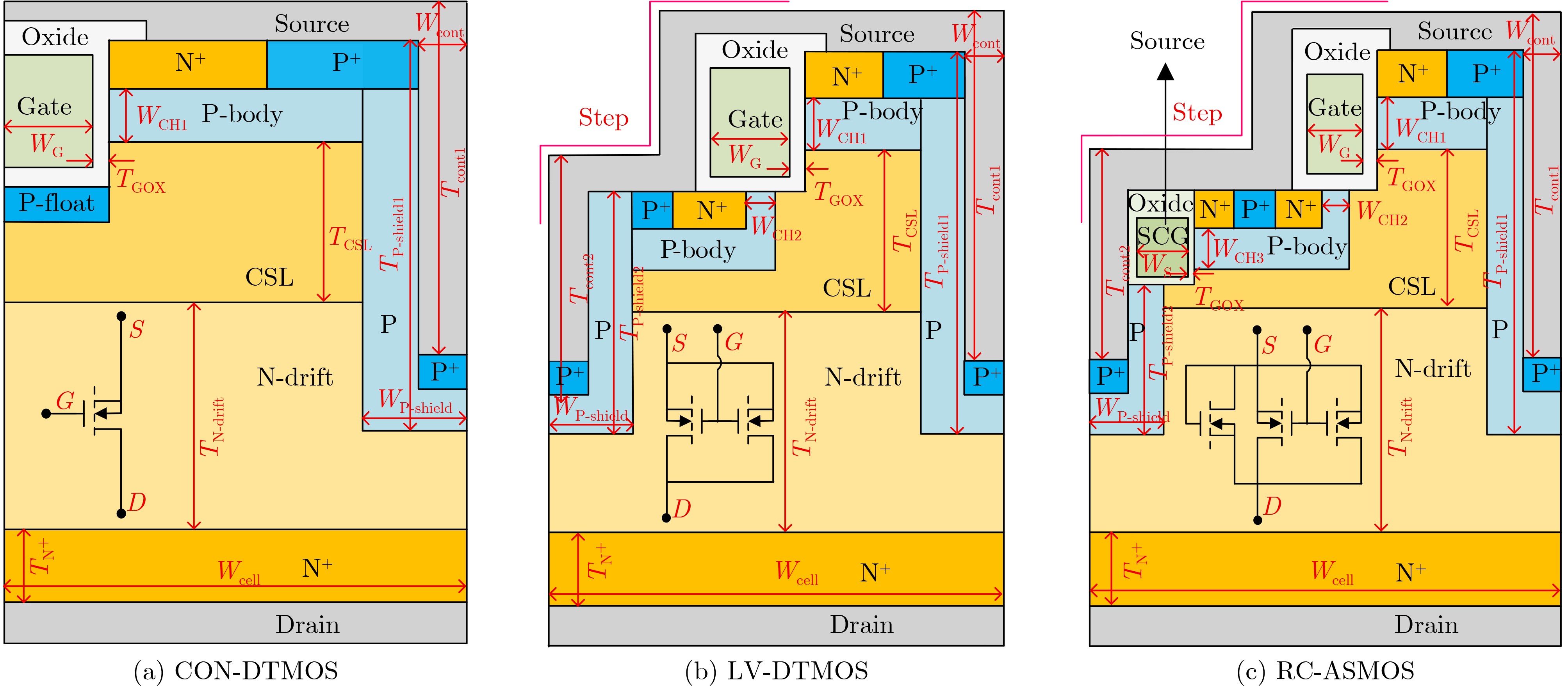
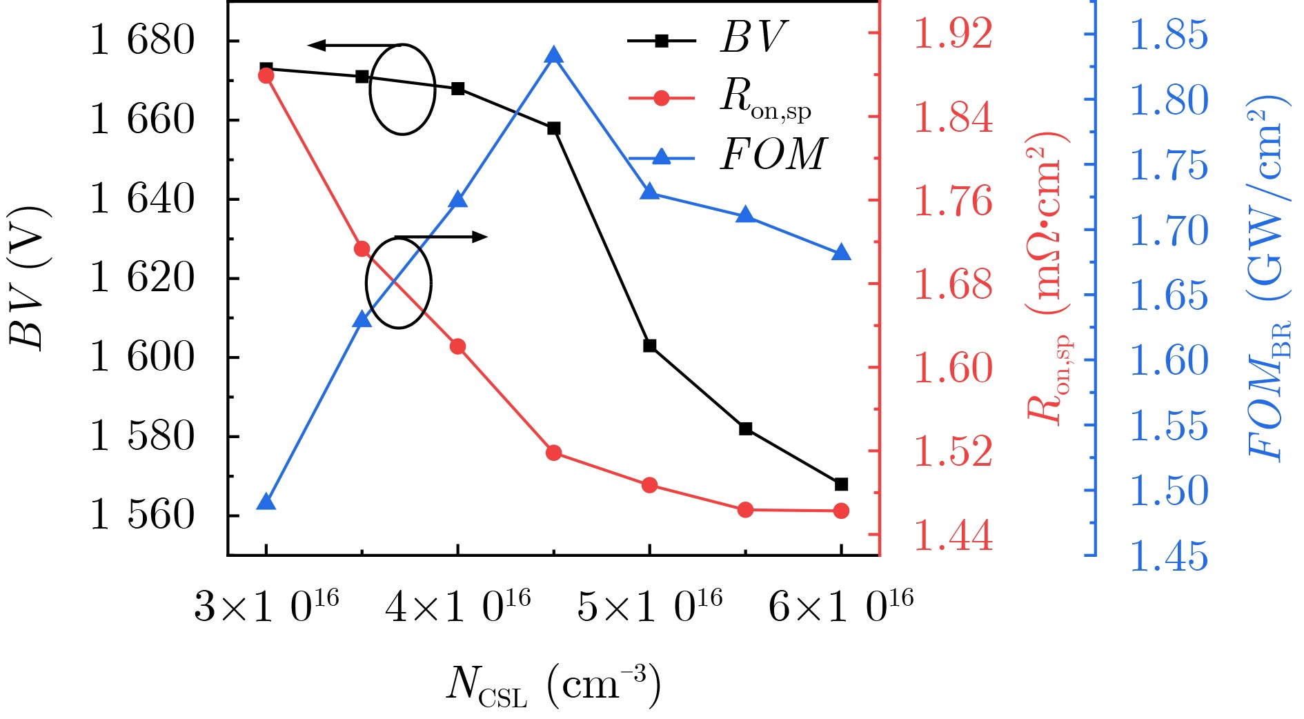
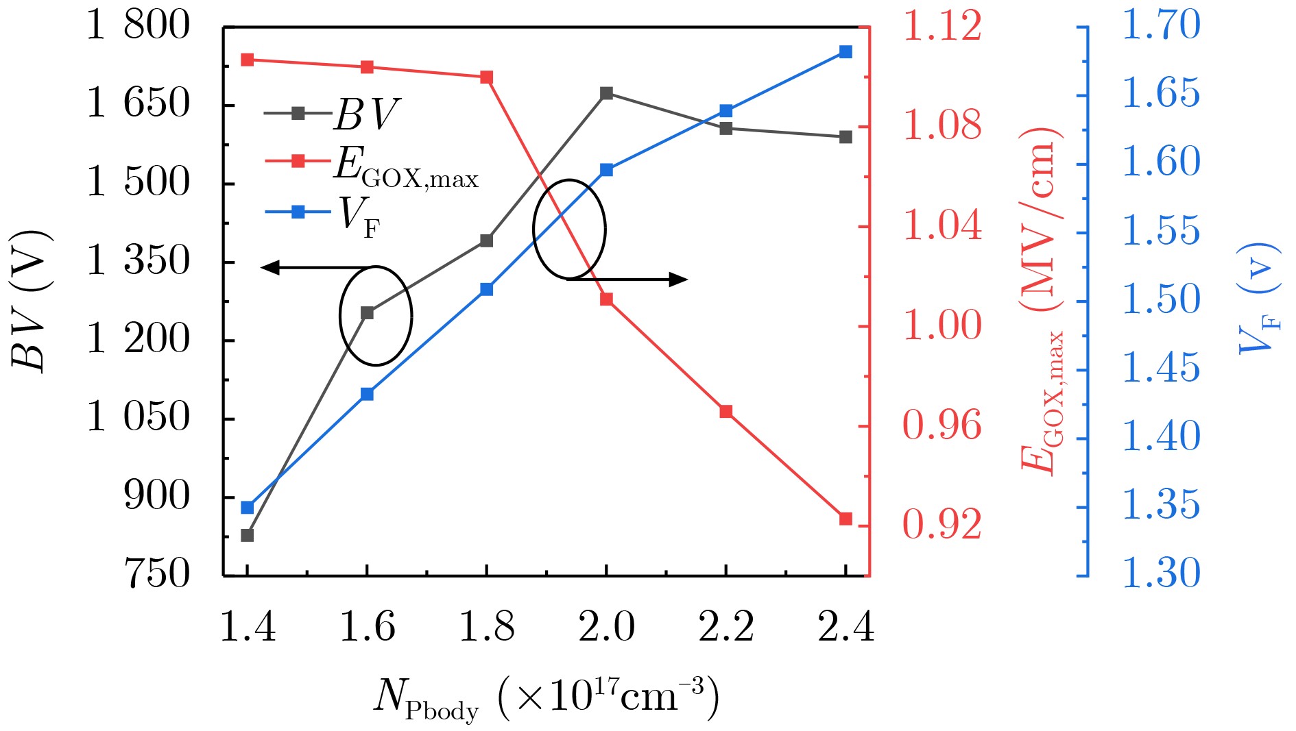
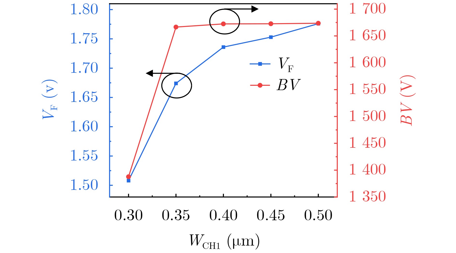
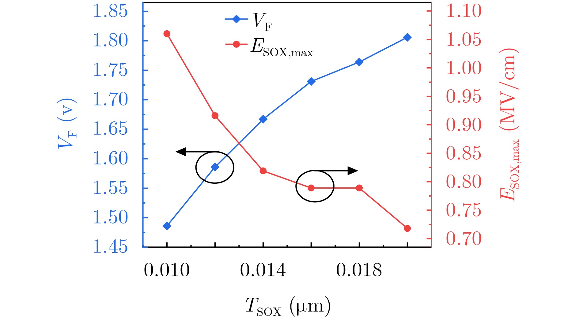
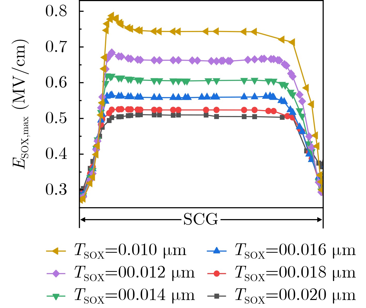
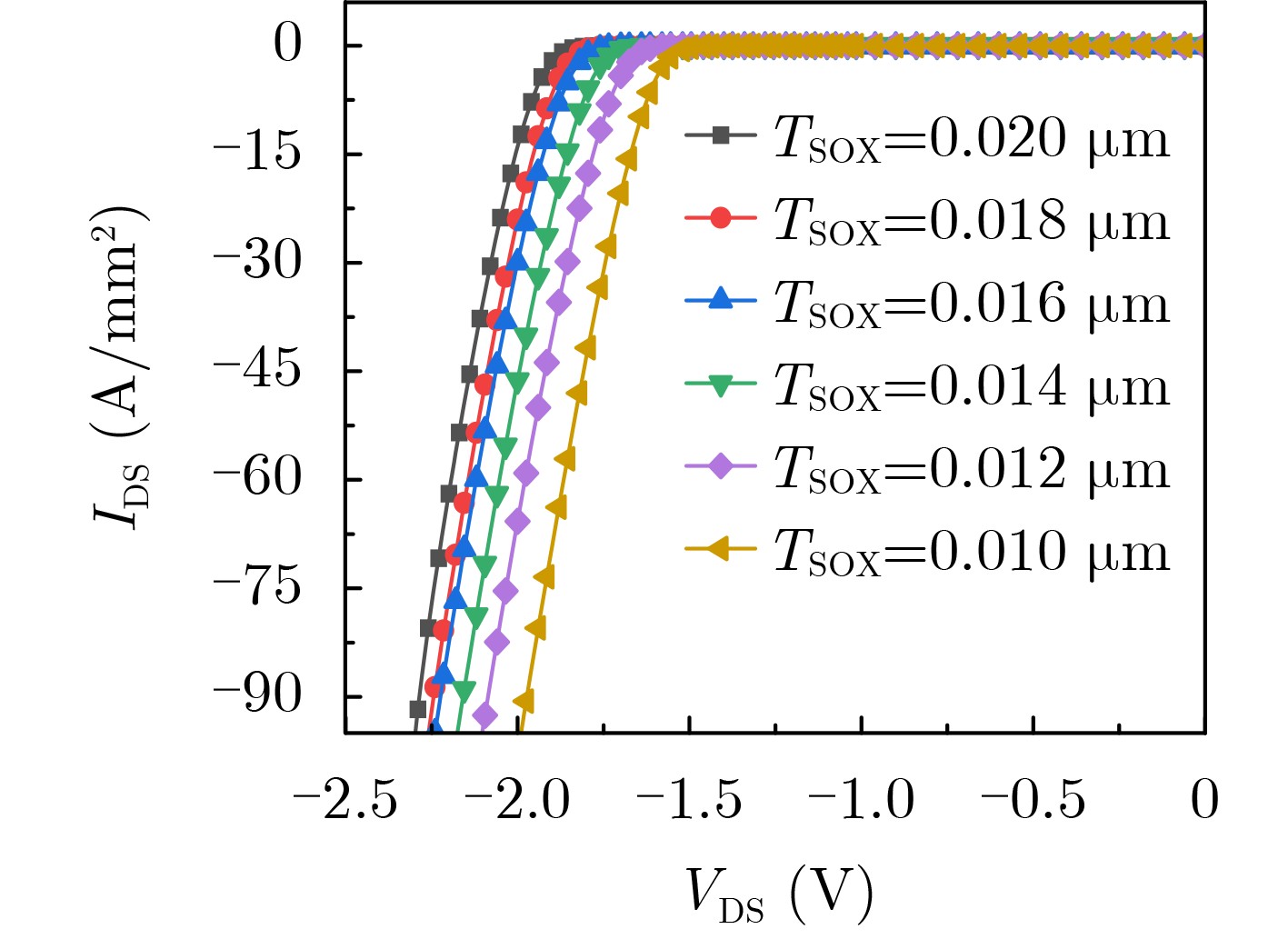
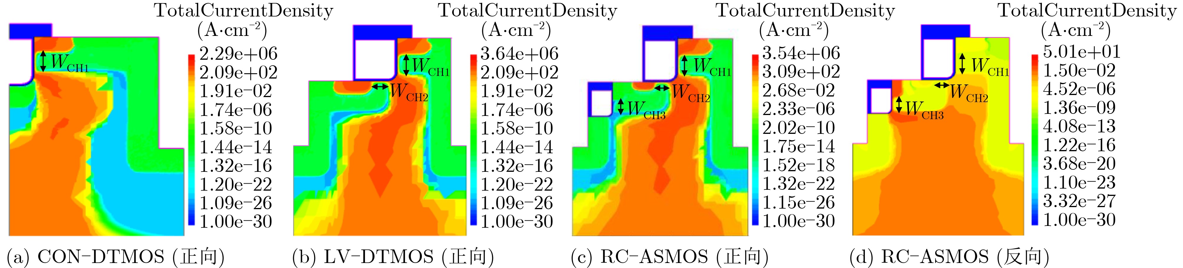
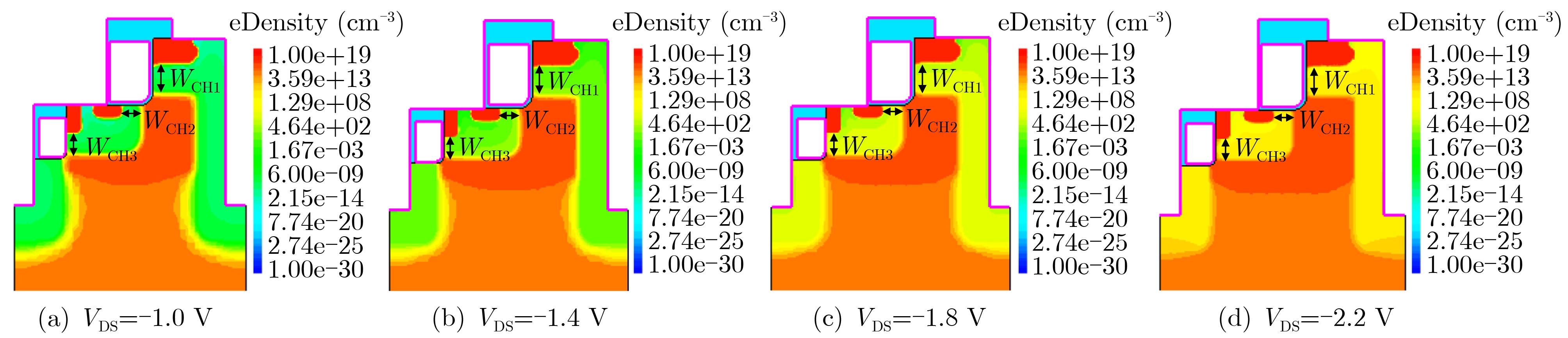
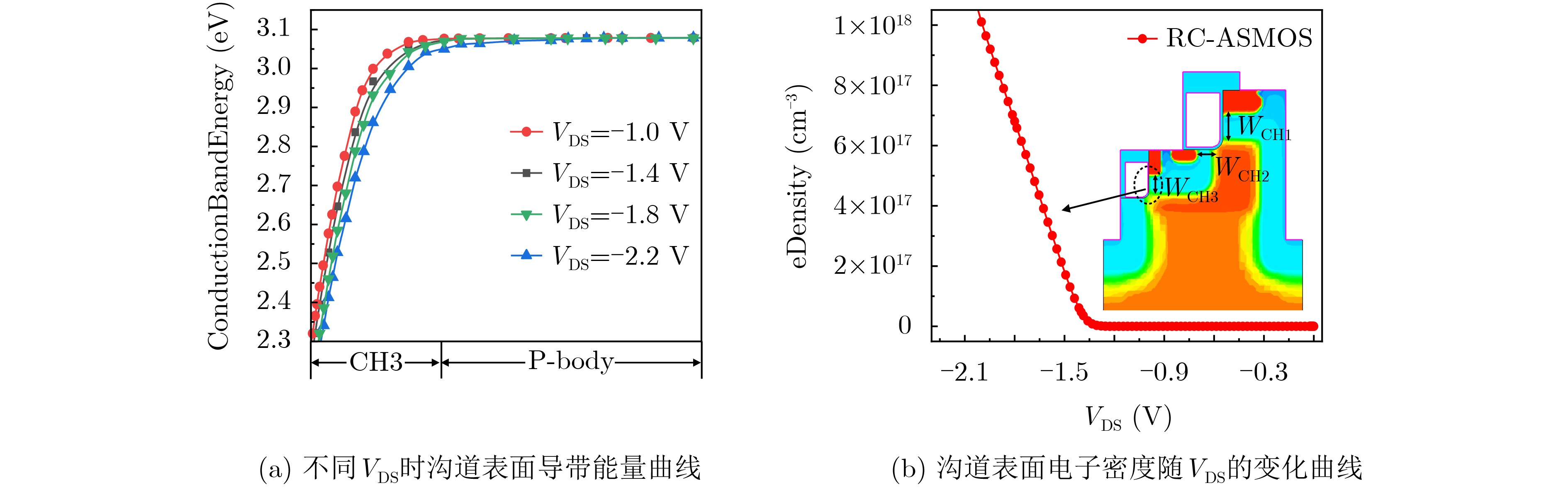
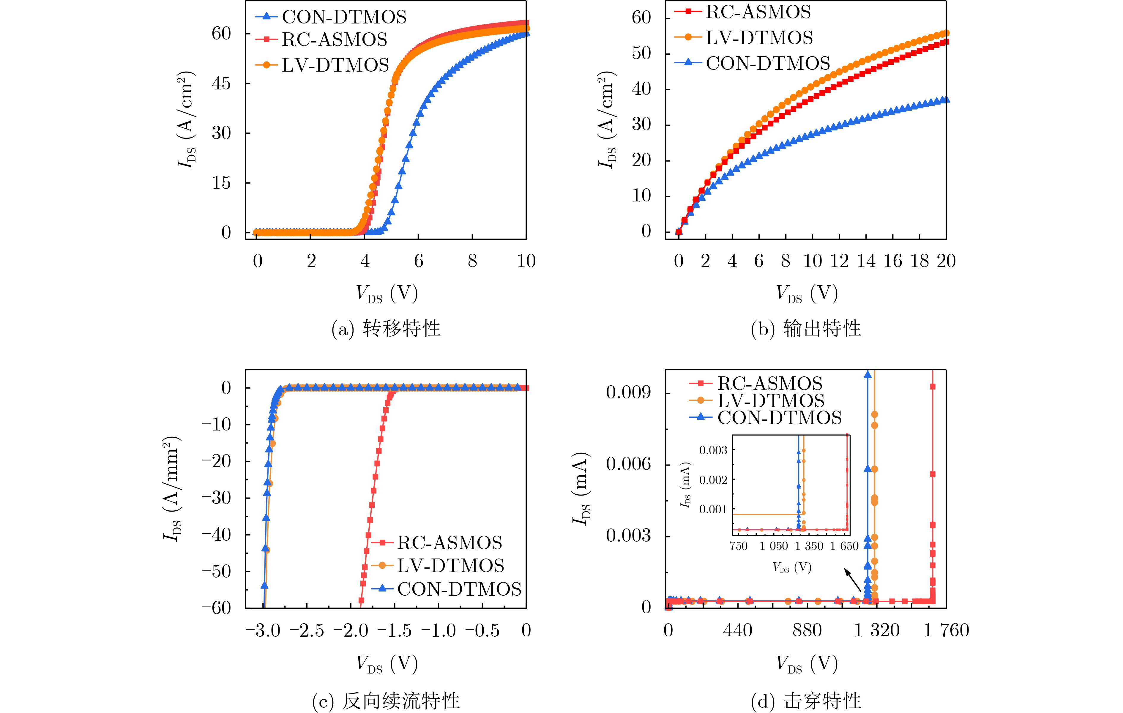
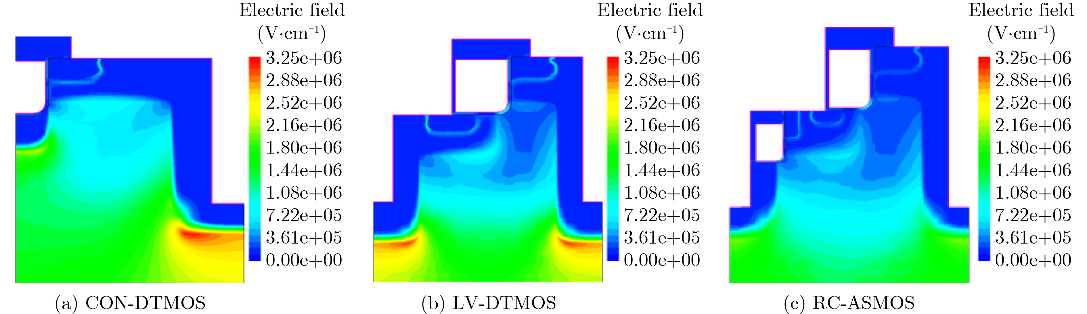
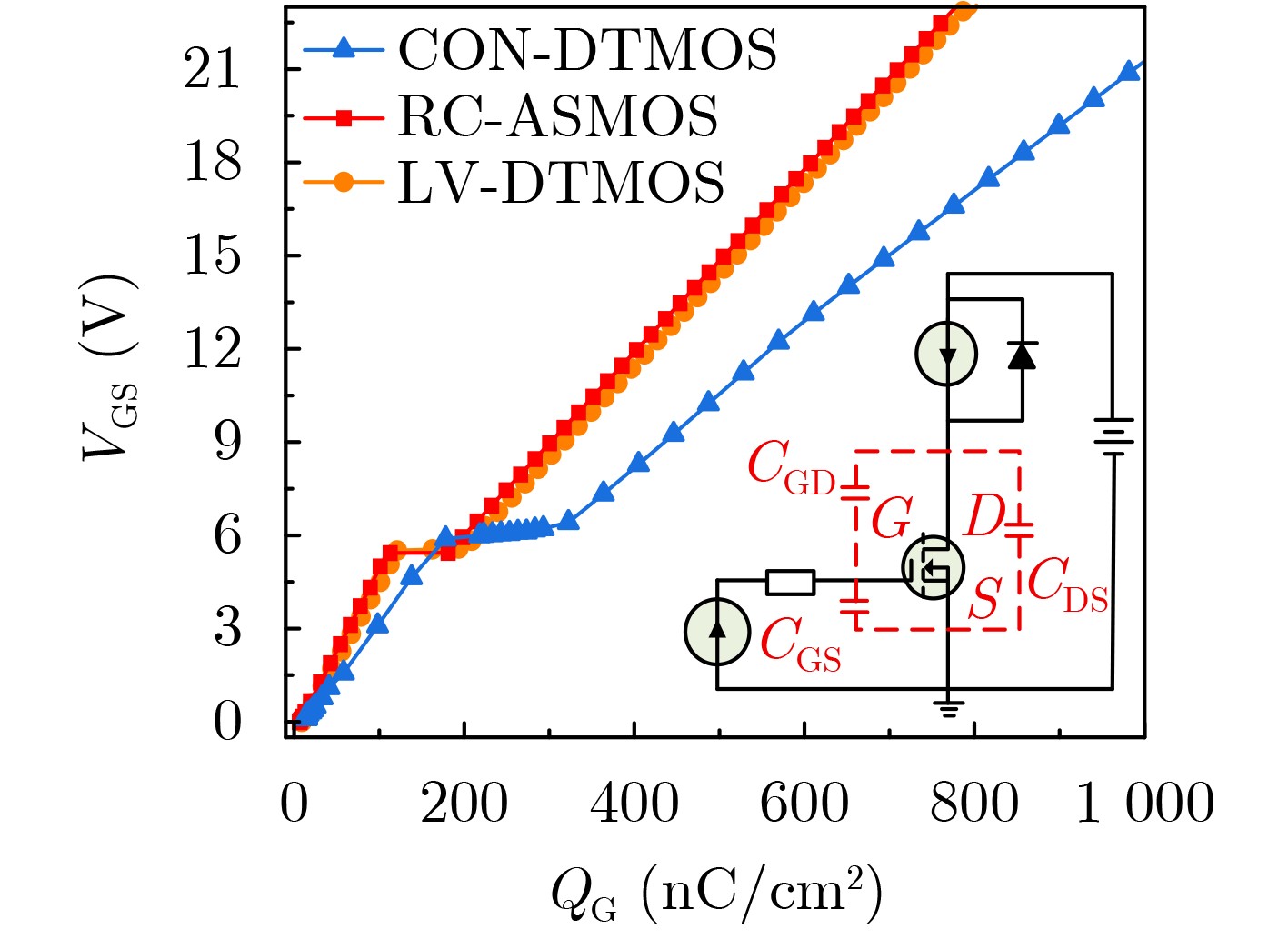
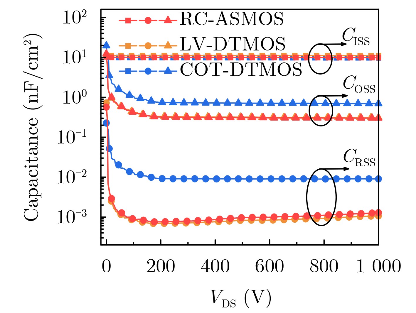
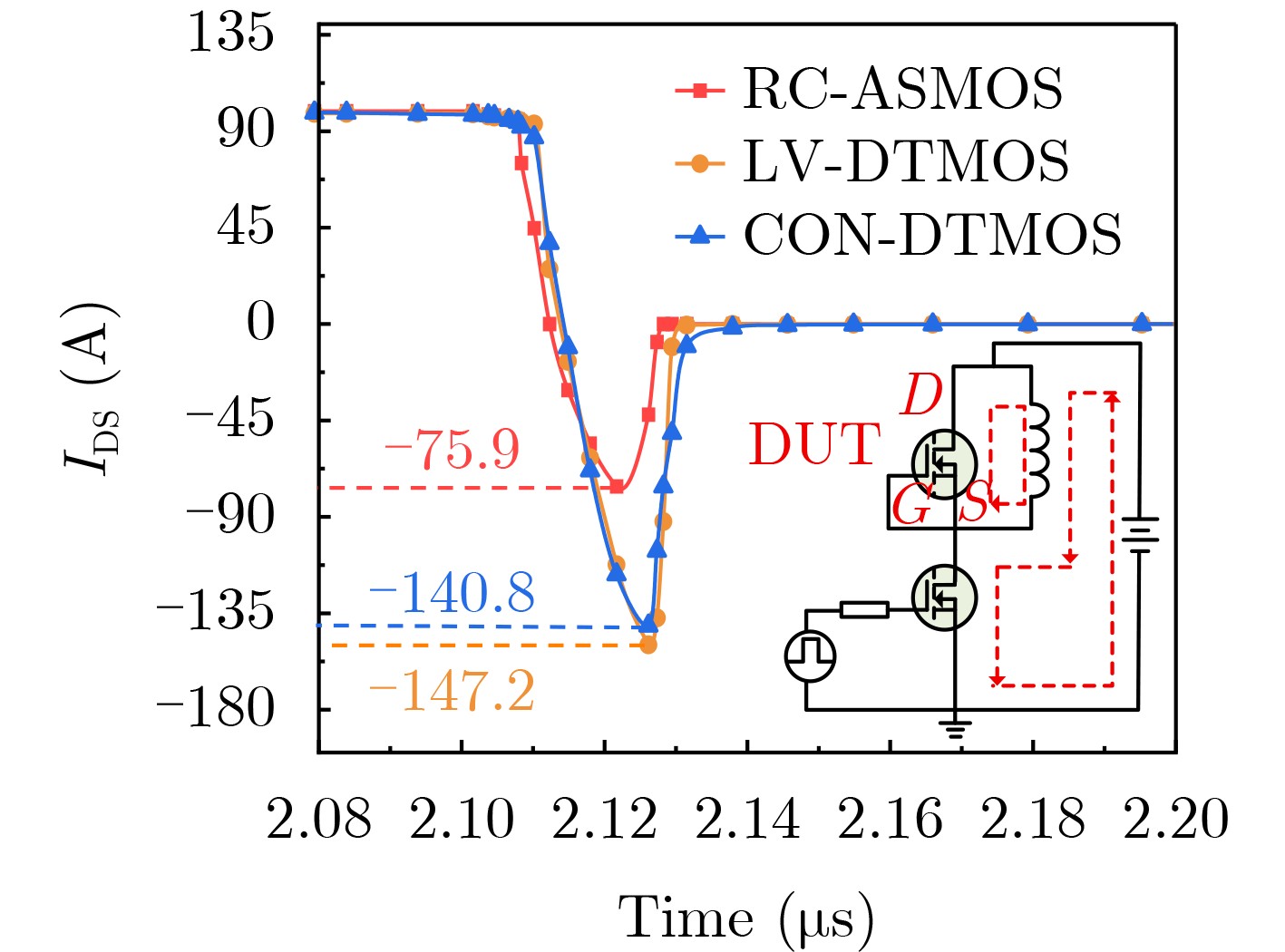
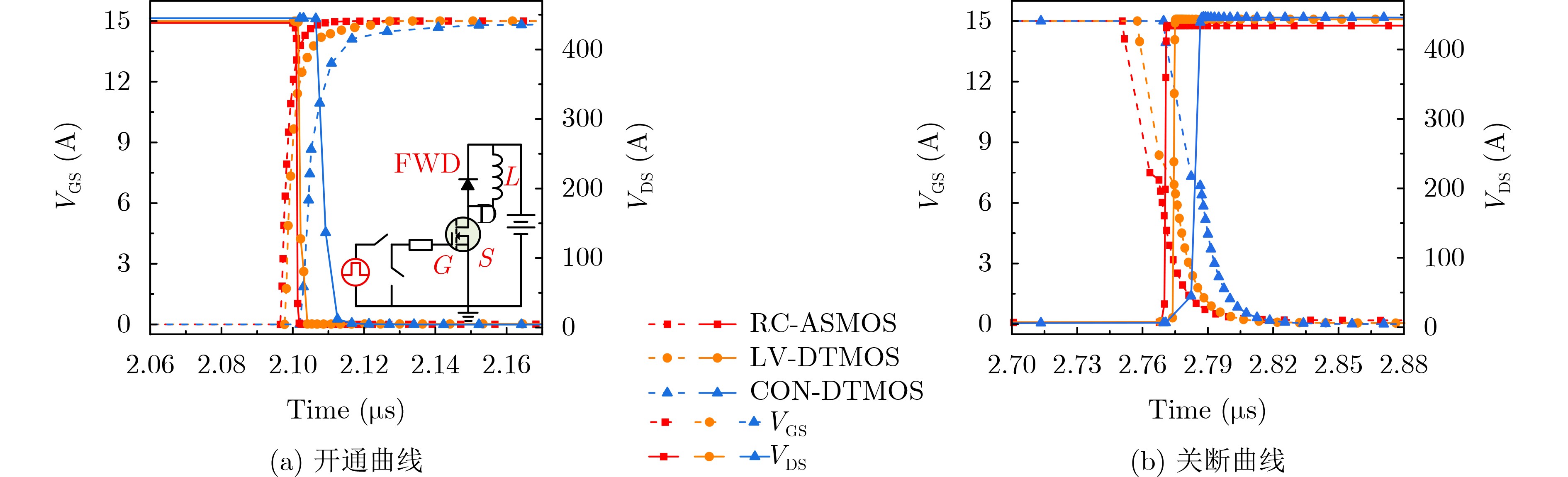
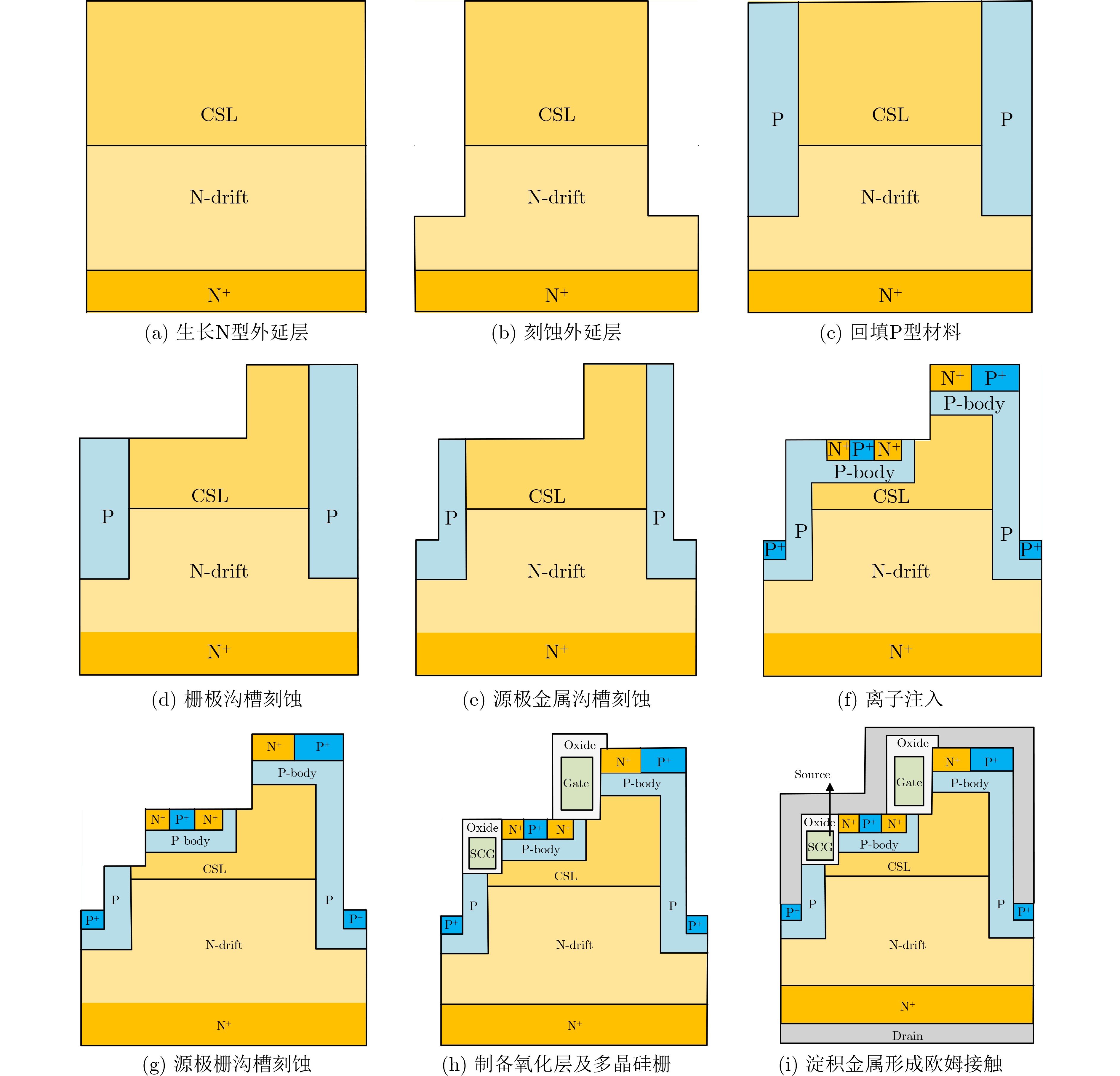
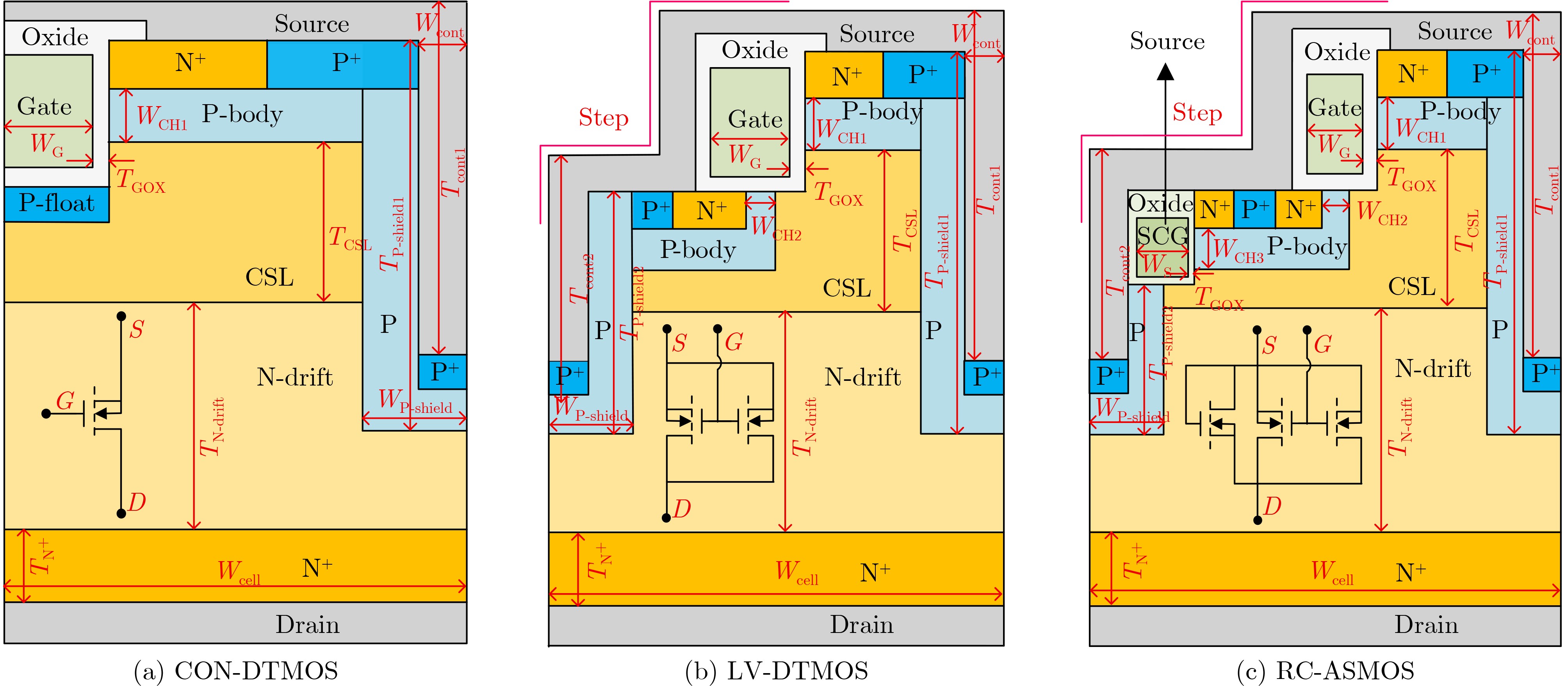
Objective Featuring superior material properties including high thermal conductivity, high critical breakdown electric field, and high electron saturation velocity, 4H-SiC MOSFETs break through the performance bottlenecks of conventional silicon-based MOSFETs and satisfy the core requirements of power electronic systems for high frequency, miniaturization, and high efficiency. Among them, the double-trench 4H-SiC MOSFET (DT-MOS) developed by ROHM has been widely adopted in power electronic systems such as three-phase inverters for new energy vehicles and wind power generation. Nevertheless, the conventional DT-MOS (CON-DTMOS) suffers from prominent performance limitations. Restricted by the wide-bandgap characteristics of 4H-SiC materials, its parasitic body diode exhibits poor reverse freewheeling capability and high conduction loss, accompanied by severe bipolar degradation. In addition, the drawbacks of CON-DTMOS, including large on-resistance, high gate-drain capacitance, and excessive reverse recovery charge, further limit its application scope. To address the aforementioned performance deficiencies of CON-DTMOS, this paper proposes two novel device structures, namely LV-DTMOS and RC-ASMOS. By introducing planar channels and reverse channels, the proposed structures reduce the on-resistance and reverse turn-on voltage and effectively suppress the bipolar degradation induced by the body diode. Meanwhile, the optimized trench structure shields the gate-drain capacitance and improves the dynamic characteristics of the device. Consequently, the optimized 4H-SiC MOSFET with comprehensive and balanced performance is realized, which completely eliminates the bipolar degradation effect and lays a solid foundation for the reliable application of 4H-SiC MOSFETs in high-frequency power electronic scenarios. Methods This paper carries out device structure design and parameter optimization based on the Sentaurus TCAD simulation platform. Taking the conventional double-trench 4H-SiC MOSFET (CON-DTMOS) as the research baseline, a novel LV-DTMOS structure with integrated Lateral-Vertical channels is firstly designed. On this basis, an asymmetric stepped RC-ASMOS with embedded reverse channels is further proposed through structural optimization.The forward channels CH1 and CH2 can significantly reduce the on-resistance and improve the chip integration level. Moreover, the CH2 integrated at the trench bottom can shield the gate-drain coupling capacitance, thereby enhancing the dynamic performance of the device. Meanwhile, the embedded reverse channel CH3 can be turned on at a low reverse turn-on voltage through an ultra-thin oxide layer prior to the intrinsic body diode. This avoids the electron-hole recombination process and fundamentally eliminates the bipolar degradation effect.To improve the accuracy and reliability of simulation results, multiple critical physical models are adopted in the simulation process, including the incomplete ionization model, bandgap narrowing model, avalanche effect model, and high-field mobility saturation model. Furthermore, an interface charge model is introduced to account for the influence of interface state charges at the SiC/SiO2 interface on channel mobility. The comprehensive application of the above multi-physical models enables the establishment of a simulation model that is highly consistent with the physical behaviors of practical devices, which provides a reliable support for subsequent device characteristic analysis and parameter optimization. Results and Discussions Simulation results indicate that the RC-ASMOS achieves optimal comprehensive performance under the structural and doping parameters of a CSL layer doping concentration of 4.5×1017 cm–3, a reverse channel width of 0.35 μm, a source oxide thickness of 0.012 μm, and a P-body doping concentration of 2.0×1019 cm–3. Compared with the conventional CON-DTMOS, the optimized RC-ASMOS exhibits substantial improvements in overall performance. The specific on-resistance of the RC-ASMOS is reduced by 29.1%, and the forward voltage drop is decreased from 2.8 V to 1.6 V, corresponding to a reduction of 42.9%. In addition, the proposed device effectively optimizes the internal electric field distribution and alleviates the electric field crowding effect, leading to a 36.5% enhancement in breakdown voltage ( Fig. 11 ,Fig. 12 ). Benefiting from the CH2 integrated at the trench bottom, the gate-drain coupling effect is effectively weakened, which significantly reduces the gate-drain capacitance and lowers the gate charge by 53.9% (Fig. 13 ,Fig. 14 . Furthermore, the RC-ASMOS realizes unipolar reverse freewheeling through the embedded reverse channel CH3, which suppresses the minority carrier storage effect and greatly improves the reverse recovery characteristics. The reverse recovery charge is reduced by 46.2%, and the peak reverse current is remarkably decreased (Fig. 15 ). Consequently, the proposed RC-ASMOS possesses excellent static conduction performance and high-frequency dynamic switching performance simultaneously.Conclusions Based on the conventional double-trench 4H-SiC MOSFET (CON-DTMOS), this paper conducts device design, parameter optimization, and performance verification using the Sentaurus TCAD simulation platform. Firstly, an LV-DTMOS structure with integrated planar-vertical channels is simulated. On this basis, structural optimization is further performed, and a novel RC-ASMOS device with embedded reverse channels is proposed. By optimizing the internal carrier transport paths, the RC-ASMOS achieves significant improvements in both static and dynamic device performance.Thanks to the unique reverse channel, the RC-ASMOS can be turned on for reverse freewheeling prior to the parasitic body diode, which avoids the internal electron-hole recombination process and fundamentally eliminates the bipolar degradation effect. Meanwhile, the RC-ASMOS remarkably reduces the gate-drain overlapping area, yielding a substantial improvement in dynamic characteristics. Overall, the proposed RC-ASMOS realizes comprehensive performance optimization and effectively breaks through the performance limitations of traditional 4H-SiC MOSFETs. -
表 1 三种器件结构的主要结构参数
参数 CON-DTMOS(半元胞) LV-DTMOS RC-ASMOS TN-drift (μm) 10.0 10.0 10.0 NN-drift (cm–3) 5.0×10¹⁵ 5.0×10¹⁵ 5.0×10¹⁵ TCSL (μm) 2.0 2.0 2.0 NCSL (cm–3) 4.5×10¹⁶ 4.5×10¹⁶ 4.5×10¹⁶ NP+ (cm–3) 1.0×10¹⁹ 1.0×10¹⁹ 1.0×10¹⁹ NN+ (cm–3) 1.0×10¹⁹ 1.0×10¹⁹ 1.0×10¹⁹ NP-body (cm–3) 2.0×10¹⁷ 2.0×10¹⁷ 2.0×10¹⁷ TGOX (μm) 0.05 0.05 0.05 TSOX (μm) / / 0.012 TP-shield2 (μm) / 2.0 1.2 TP-shield1 (μm) 3.0 3.0 3.0 WP-shield (μm) 0.7 0.7 0.7 Tcont1 (μm) 2.5 2.5 2.5 Tcont2 (μm) 1.5 1.5 1.5 Wcont (μm) 0.3 0.3 0.3 WS (μm) / / 0.4 WCH3 (μm) / / 0.35 WCH2 (μm) / 0.3 0.3 WCH1 (μm) 0.3 0.3 0.3 Wcell (μm) 3.5 3.5 3.5 WG (μm) 0.45 0.8 0.6  下载: 导出CSV
表 2 三种器件结构的主要特性对比
电学特性 CON-DTMOS LV-DTMOS RC-ASMOS Ron,sp (mΩ·cm2) 2.13 1.46 1.51 VF (V) 2.8 2.8 1.6 BV (V) 1226 1305 1673 QGD (nC/cm2) 148.1 72.2 68.3 FOMRQ (mΩ·nC) 315.5 105.4 103.1 QRR (μC/cm2) 0.26 0.26 0.14 IRRM (A) 147.2 140.8 75.9 TON (μs) 0.0154 0.0055 0.0045 TOFF (μs) 0.020 0.0153 0.0143
下载: 导出CSV
-
[1] 商世广, 郭雄雄, 张雨, 等. 一种三层EPI结构SGT MOSFET设计[J]. 西安邮电大学学报, 2023, 28(4): 36–43. doi: 10.13682/j.issn.2095-6533.2023.04.005.SHANG Shiguang, GUO Xiongxiong, ZHANG Yu, et al. Design of SGT MOSFET with three-layer EPI structure[J]. Journal of Xi’an University of Posts and Telecommunications, 2023, 28(4): 36–43. doi: 10.13682/j.issn.2095-6533.2023.04.005. [2] ZERROUMDA B, FERHATI H, DJEFFAL F, et al. A novel high-performance junctionless 4H-SiC trench MOSFET with improved switching characteristics[J]. Microelectronic Engineering, 2023, 277: 112011. doi: 10.1016/j.mee.2023.112011. [3] 邱一武, 梁迪, 殷亚楠, 等. SiC功率MOSFET单粒子效应与加固技术研究进展[J]. 物理学报, 2025, 74(13): 136103. doi: 10.7498/aps.74.20250273.QIU Yiwu, LIANG Di, YIN Yanan, et al. Research progress of single event effect and reinforcement technology of SiC power metal-oxide-semiconductor field-effect transistors[J]. Acta Physica Sinica, 2025, 74(13): 136103. doi: 10.7498/aps.74.20250273. [4] BUFFOLO M, FAVERO D, MARCUZZI A, et al. Review and outlook on GaN and SiC power devices: Industrial state-of-the-art, applications, and perspectives[J]. IEEE Transactions on Electron Devices, 2024, 71(3): 1344–1355. doi: 10.1109/TED.2023.3346369. [5] 方绍明, 李宏达, 高源. 基于双侧P型柱与电流扩展层协同设计的1 200 V沟槽型SiC MOSFET性能优化与栅氧电场分析[J]. 电子与信息学报, 2026, 48(8): 3682–3690. doi: 10.11999/JEIT260164.FANG Shaoming, LI Hongda, and GAO Yuan. Performance optimization and gate oxide electric field analysis of 1200V trench SiC MOSFET based on PCL-CSL collaborative design[J]. Journal of Electronics & Information Technology, 2026, 48(8): 3682–3690. doi: 10.11999/JEIT260164. [6] SHE Xu, HUANG A Q, LUCÍA Ó, et al. Review of silicon carbide power devices and their applications[J]. IEEE Transactions on Industrial Electronics, 2017, 64(10): 8193–8205. doi: 10.1109/TIE.2017.2652401. [7] 谭会生, 刘帅, 戴小平. 一种新型阶梯栅多沟道SiC MOSFET结构[J]. 半导体技术, 2025, 50(11): 1114–1121,1127. doi: 10.13290/j.cnki.bdtjs.2025.11.003.TAN Huisheng, LIU Shuai, and DAI Xiaoping. A novel stepped gate multi-channel SiC MOSFET structure[J]. Semiconductor Technology, 2025, 50(11): 1114–1121,1127. doi: 10.13290/j.cnki.bdtjs.2025.11.003. [8] YANG Juefei, JAHDI S, YU Renze, et al. Electrothermal power cycling to failure of discrete planar, symmetrical double-trench and asymmetrical trench SiC MOSFETs[J]. IEEE Open Journal of Power Electronics, 2023, 4: 887–899. doi: 10.1109/OJPEL.2023.3326909. [9] 马超, 陈伟中, 张波. 集成肖特基二极管的分裂栅碳化硅(SiC)MOSFET器件[J]. 电子与信息学报, 2025, 47(9): 3346–3352. doi: 10.11999/JEIT250180.MA Chao, CHEN Weizhong, and ZHANG Bo. A novel silicon carbide (SiC) MOSFET with schottky diode integration technology[J]. Journal of Electronics & Information Technology, 2025, 47(9): 3346–3352. doi: 10.11999/JEIT250180. [10] 高升, 章先锋, 陈秋锐, 等. 集成JFET续流二极管的低开关损耗双沟槽SiC MOSFET[J]. 电子与信息学报, 2025, 47(9): 3303–3311. doi: 10.11999/JEIT250237.GAO Sheng, ZHANG Xianfeng, CHEN Qiurui, et al. Low switching loss double trench SiC MOSFET with integrated JFET continuity diode[J]. Journal of Electronics & Information Technology, 2025, 47(9): 3303–3311. doi: 10.11999/JEIT250237. [11] SUNG W and BALIGA B J. On developing one-chip integration of 1.2 kV SiC MOSFET and JBS diode (JBSFET)[J]. IEEE Transactions on Industrial Electronics, 2017, 64(10): 8206–8212. doi: 10.1109/TIE.2017.2696515. [12] KIM J and KIM K. 4H-SiC double-trench MOSFET with side wall heterojunction diode for enhanced reverse recovery performance[J]. Energies, 2020, 13(18): 4602. doi: 10.3390/en13184602. [13] KIM D, JANG S Y, DEBOER S, et al. An optimal design for 1.2kV 4H-SiC JBSFET (junction barrier Schottky diode integrated MOSFET) with deep P-well[J]. IEEE Electron Device Letters, 2022, 43(5): 785–788. doi: 10.1109/led.2022.3162156. [14] YU Yiren, LIU Tao, MA Rongyao, et al. A novel asymmetric trench SiC MOSFET with an integrated JFET for improved reverse conduction performance[J]. IEEE Transactions on Electron Devices, 2024, 71(3): 1546–1552. doi: 10.1109/TED.2023.3333285. [15] WEI Jiaxing, WEI Zhaoxiang, FU Hao, et al. Review on the reliability mechanisms of SiC power MOSFETs: A comparison between planar-gate and trench-gate structures[J]. IEEE Transactions on Power Electronics, 2023, 38(7): 8990–9005. doi: 10.1109/TPEL.2023.3265864. [16] WEI Jin, ZHANG Meng, JIANG Huaping, et al. Low ON-resistance SiC trench/planar MOSFET with reduced OFF-state oxide field and low gate charges[J]. IEEE Electron Device Letters, 2016, 37(11): 1458–1461. doi: 10.1109/LED.2016.2609599. [17] ZHOU Xintian, GONG Hao, JIA Yunpeng, et al. SiC planar MOSFETs with built-in reverse MOS-channel diode for enhanced performance[J]. IEEE Journal of the Electron Devices Society, 2020, 8: 619–625. doi: 10.1109/JEDS.2020.3001211. [18] CHEN Weizhong, XIAO Yufan, ZHOU Yangqi, et al. A new double trench SiC MOSFET integrated multifunctional gates for improved reverse conduction performance[J]. Journal of Electronic Materials, 2025, 54(9): 7740–7751. doi: 10.1007/s11664-025-12135-8. [19] CHEN Weizhong, ZHOU Yangqi, XIAO Yufan, et al. Asymmetric trench SiC MOSFET with integrated three channels for improved performance and reliability[J]. IEEE Transactions on Device and Materials Reliability, 2025, 25(1): 95–100. doi: 10.1109/TDMR.2024.3510782. [20] HAN Zhonglin, BAI Yun, CHEN Hong, et al. A novel 4H-SiC trench MOSFET integrated with mesa-sidewall SBD[J]. IEEE Transactions on Electron Devices, 2021, 68(1): 192–196. doi: 10.1109/TED.2020.3037882. [21] CAO Xiaobo, LIU Jing, AN Yingnan, et al. A novel 4H-SiC SGT MOSFET with improved P+ shielding region and integrated schottky barrier diode[J]. Micromachines, 2024, 15(7): 933. doi: 10.3390/mi15070933. [22] YU Yiren, CHENG Zijun, HU Yi, et al. A novel asymmetric trench SiC metal-oxide-semiconductor field-effect transistor with a Poly-Si/SiC heterojunction diode for optimizing reverse conduction performance[J]. Micromachines, 2024, 15(4): 461. doi: 10.3390/mi15040461. [23] CHA K and KIM K. Asymmetric split-gate 4H-SiC MOSFET with embedded schottky barrier diode for high-frequency applications[J]. Energies, 2021, 14(21): 7305. doi: 10.3390/en14217305. -

 下载:

图(17) / 表(2)
计量
- 文章访问数: 20
- HTML全文浏览量: 3
- PDF下载量: 1
- 被引次数: 0
