




Radiation-Hardened p-GaN HEMT Featuring a Graded InGaN Channel and Schottky-Assisted Source
-
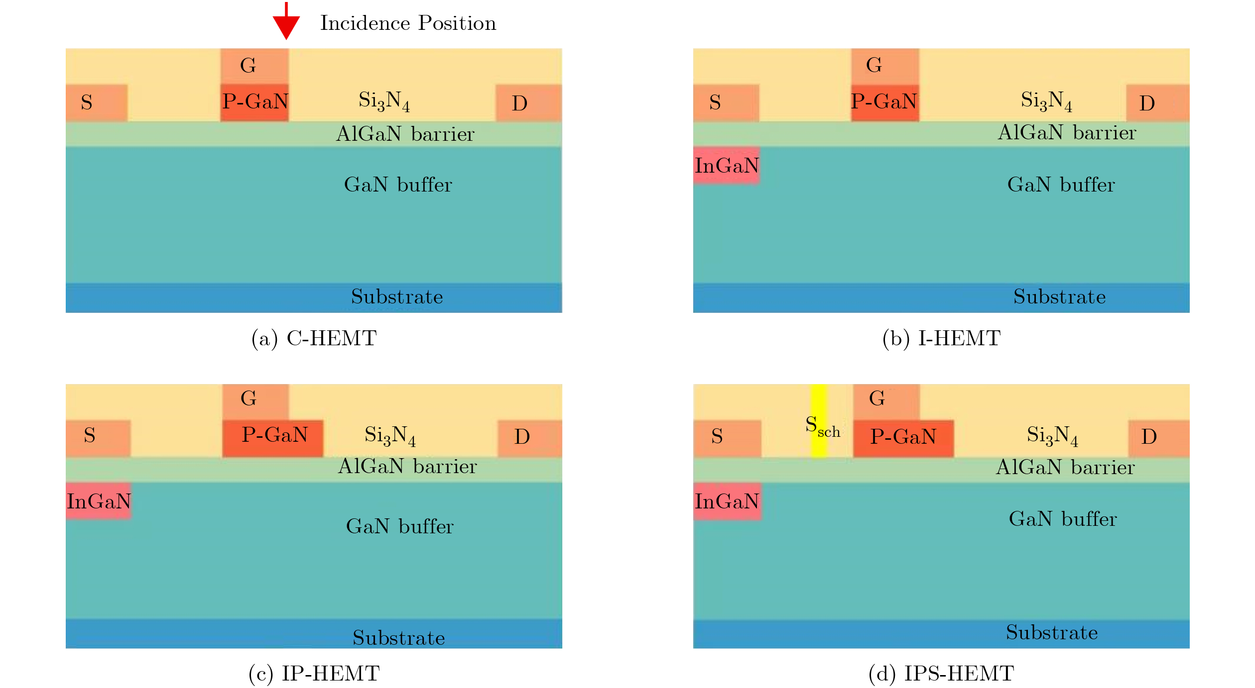
摘要: 本文提出一种集成渐变InGaN和p-GaN扩展层与肖特基源极高电子迁移率晶体管(Graded-InGaN p-GaN-Extended Schottky-Source High-Electron-Mobility Transistor, IPS-HEMT),旨在提升器件抵抗空间重离子辐照诱发单粒子烧毁(Single Event Burnout, SEB)的能力。该结构针对传统器件(Conventional High-Electron-Mobility Transistor, C-HEMT)的加固瓶颈进行了多维协同优化:首先,在源极下方引入铟(In)组分从0.8线性渐变至0.2的InGaN层,利用极化诱导的高密度二维空穴气(Two-Dimensional Hole Gas, 2DHG)促进非平衡载流子复合,从而抑制碰撞电离;其次,通过延长p-GaN栅极的覆盖范围以平滑栅漏漂移区电场;最后,在栅极与欧姆源极之间集成肖特基辅助源极,利用其附加电场实现空穴的定向高效抽取,阻断寄生双极型晶体管(Bipolar Junction Transistor, BJT)的误导通。借助TCAD数值仿真,系统优化了InGaN层长度、p-GaN扩展层掺杂浓度与长度、以及肖特基辅助源极-栅极间距等关键结构参数。结果表明,相比于传统C-HEMT,优化后的IPS-HEMT将抗SEB阈值(SEB Threshold Voltage, VSEB)大幅提升至
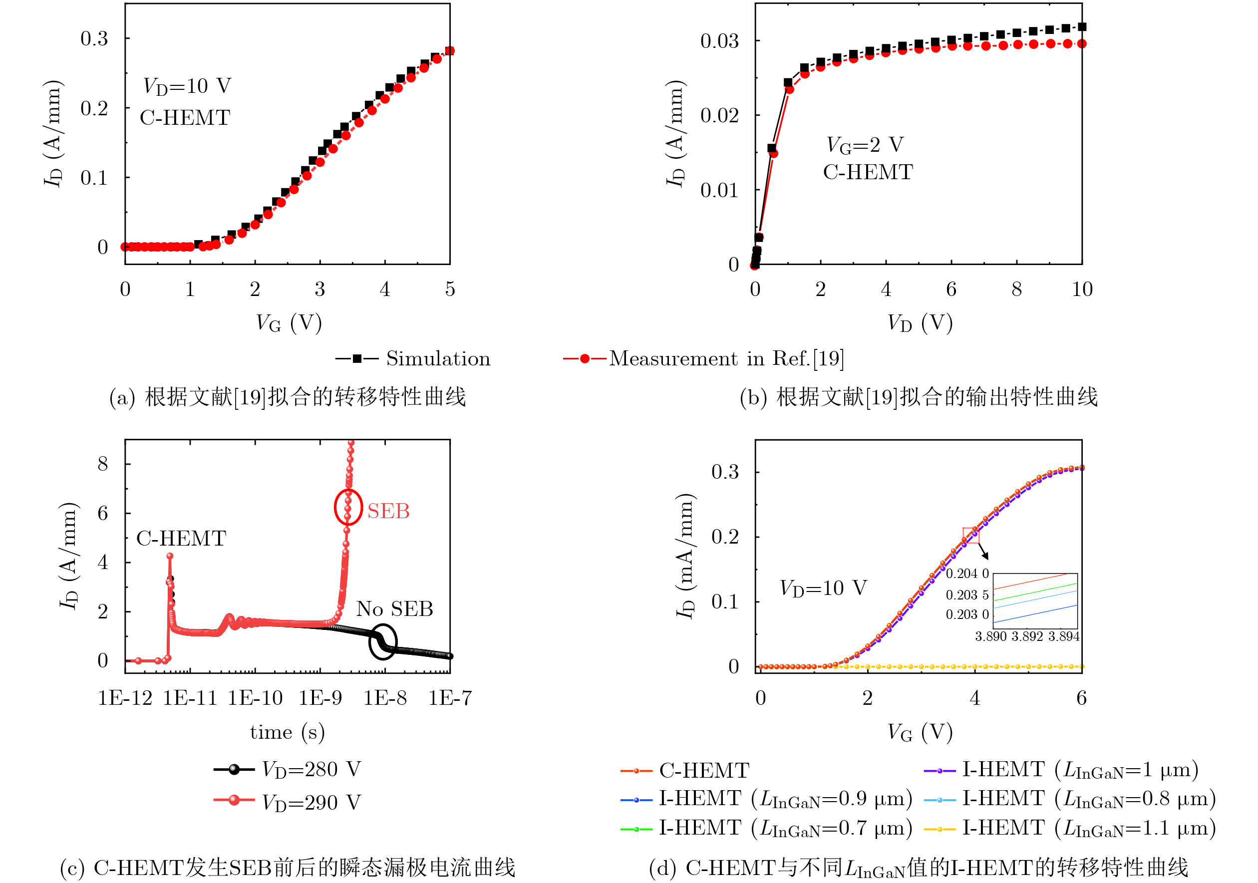
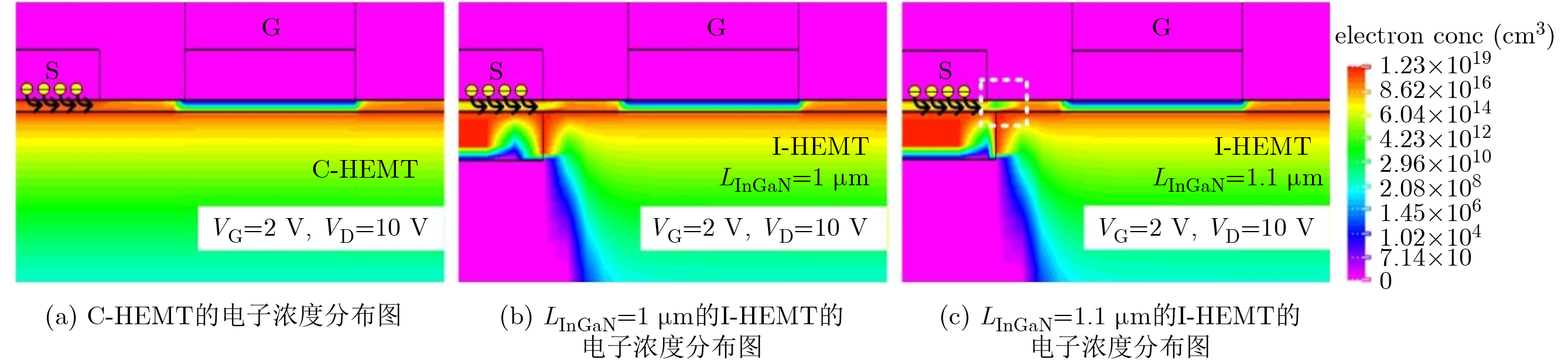
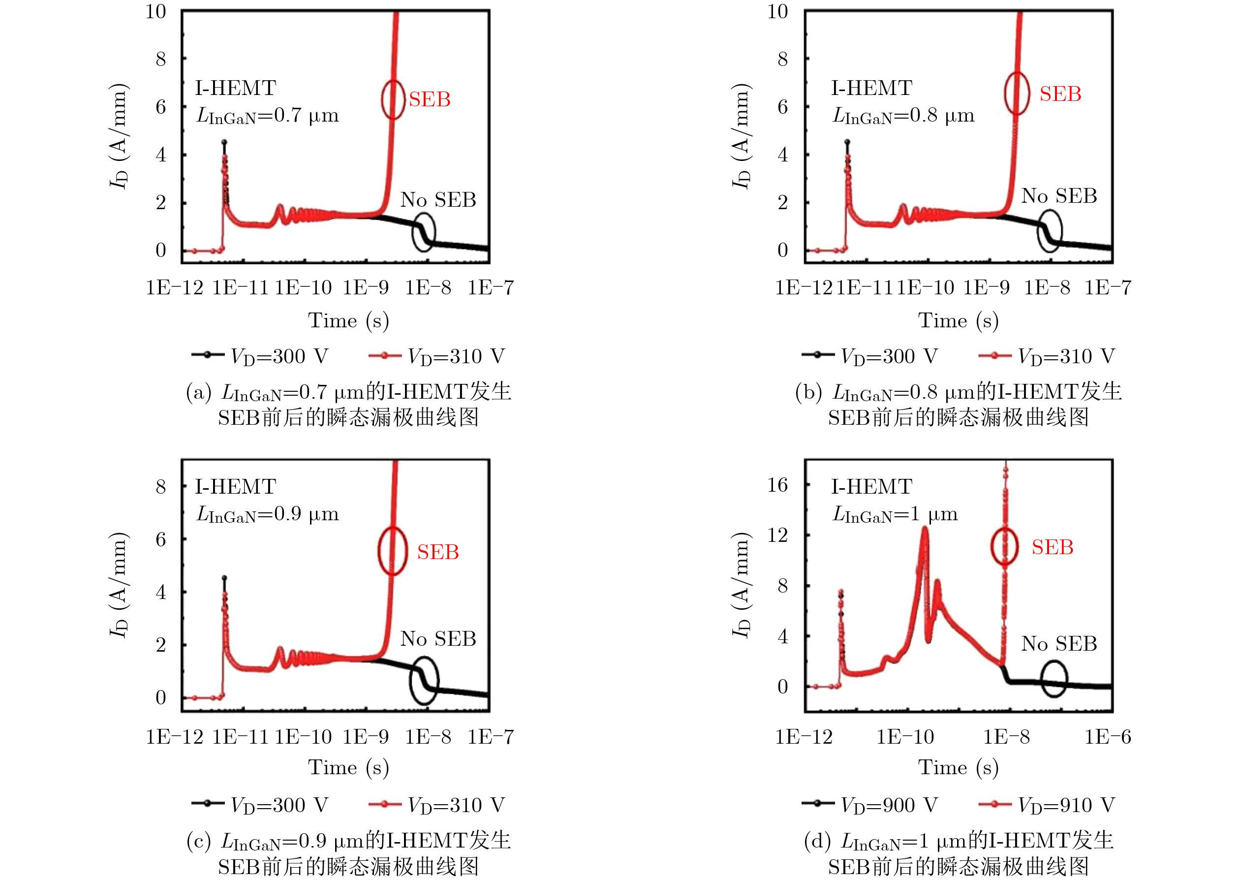
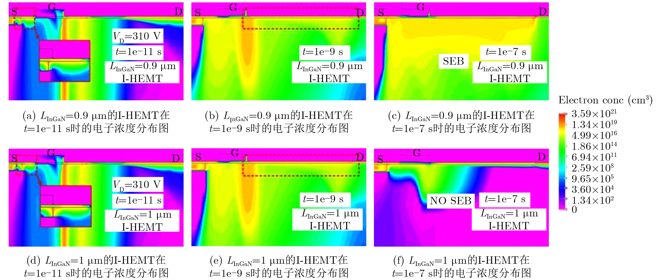
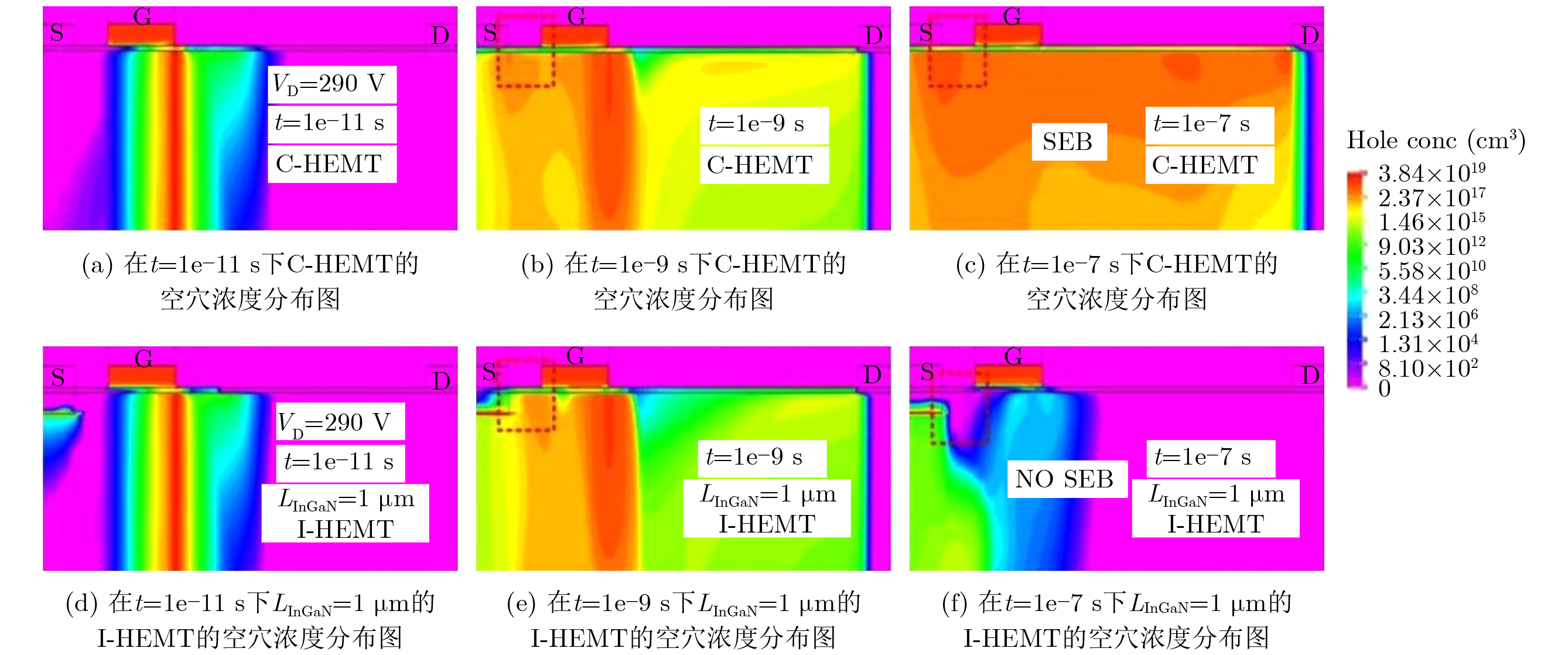
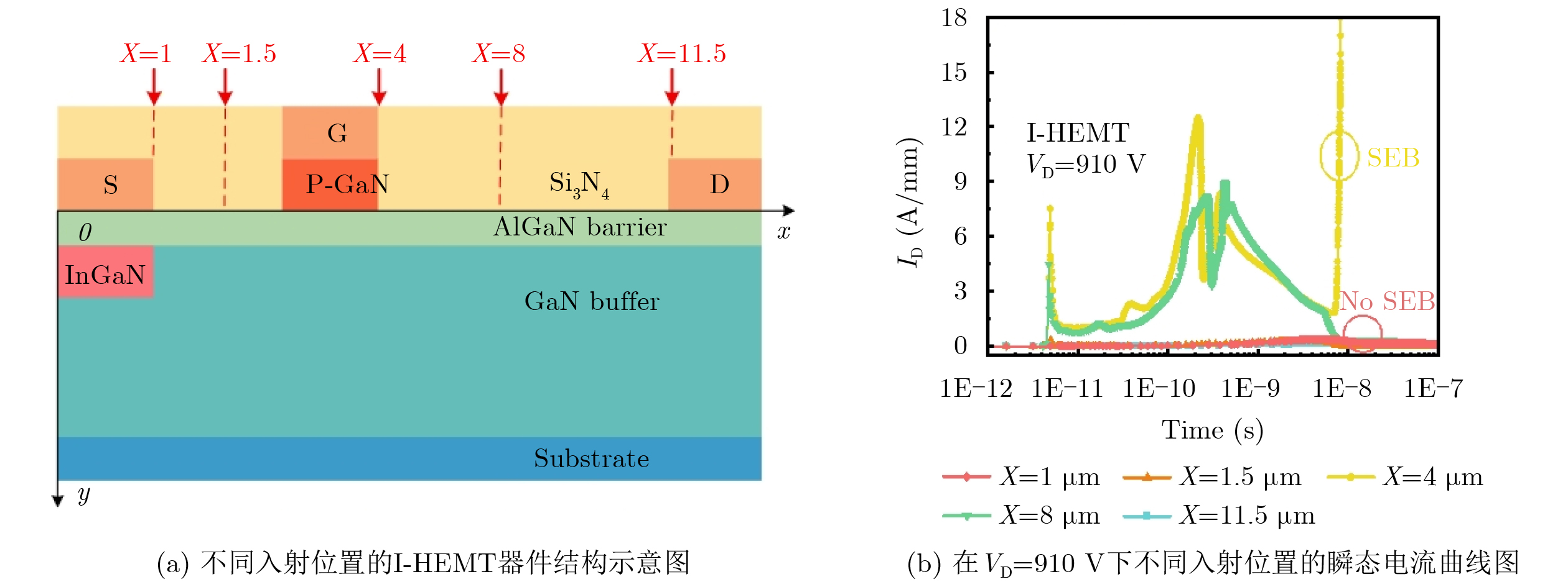
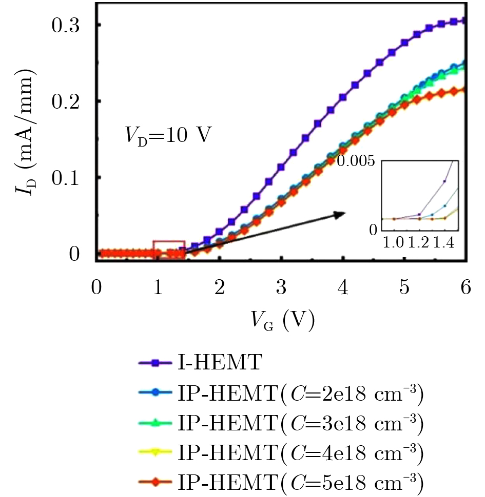
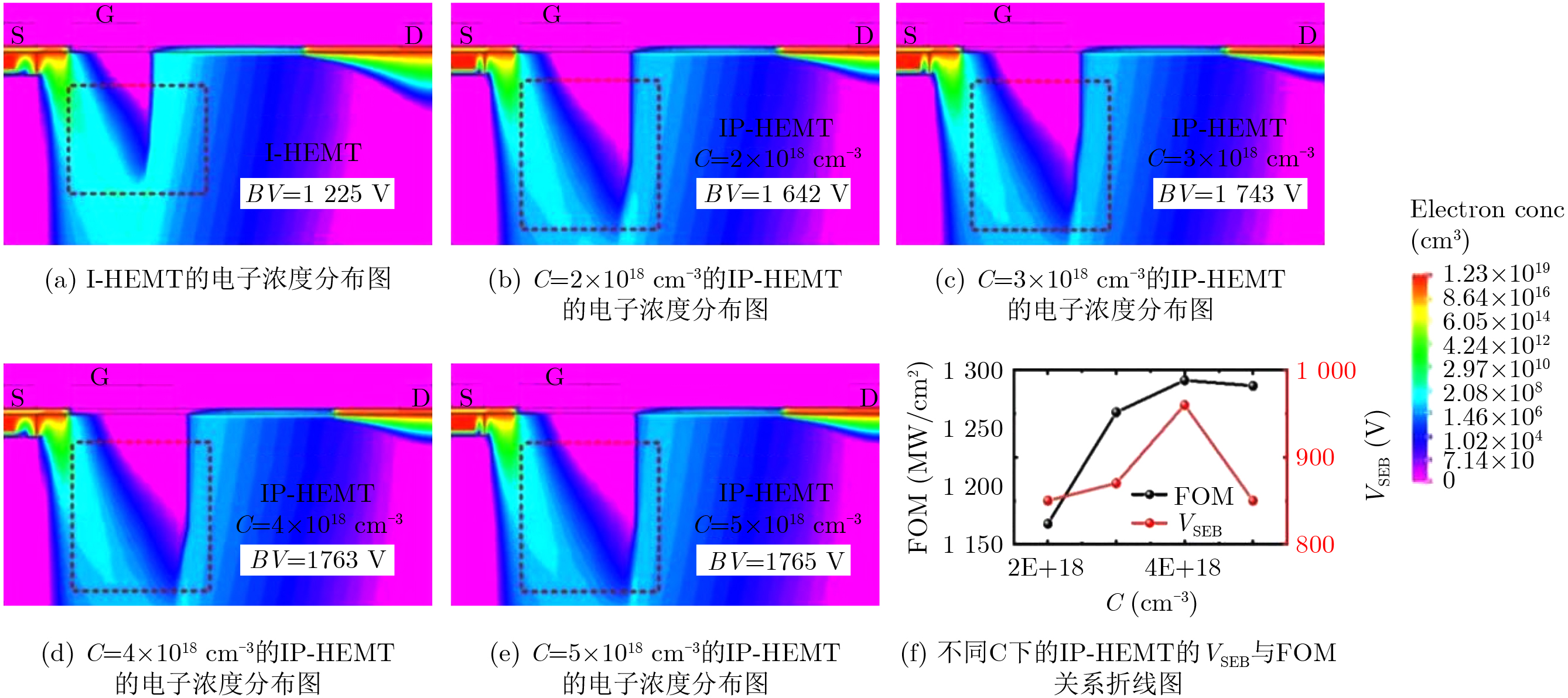
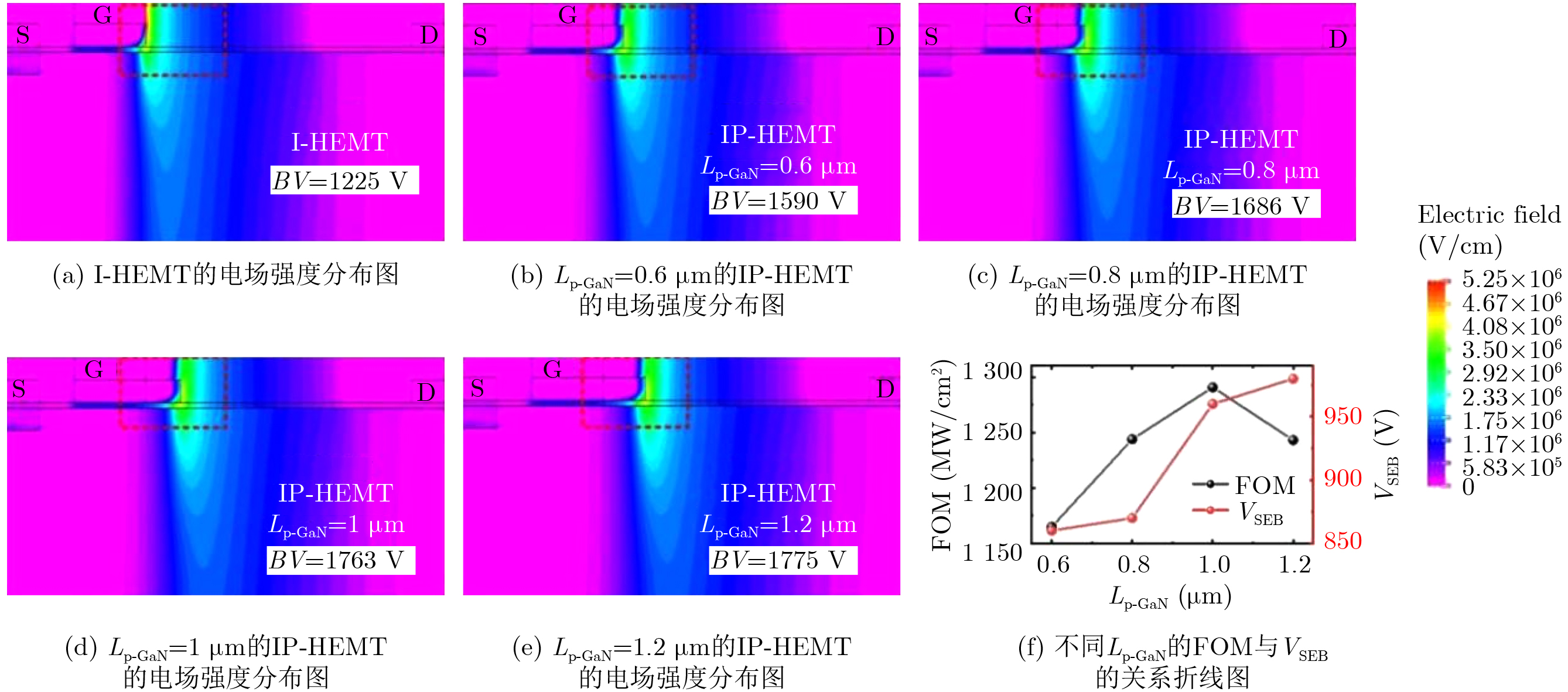
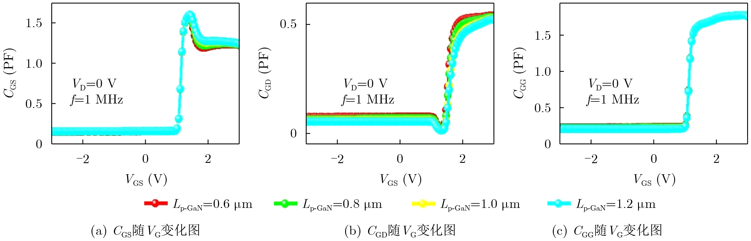
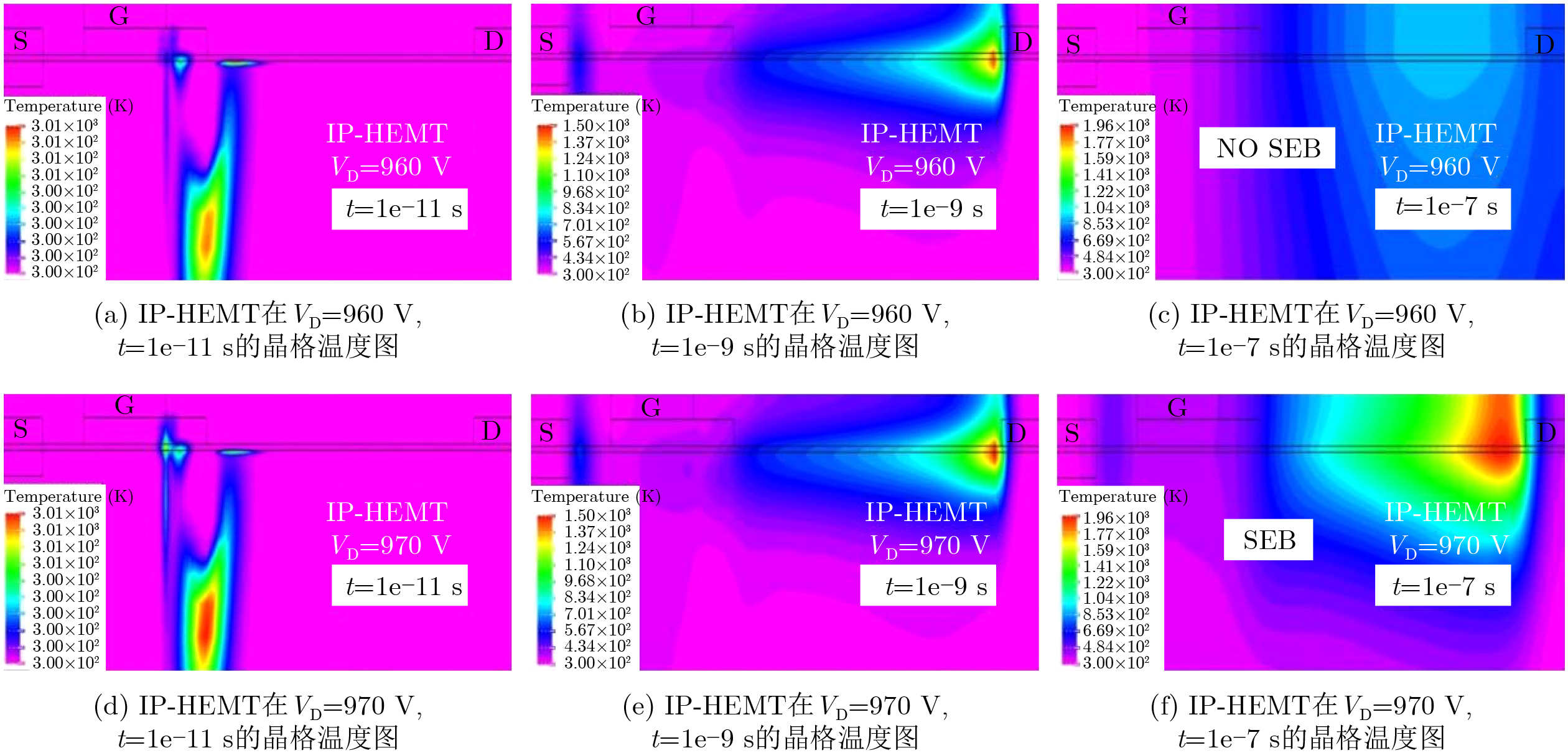
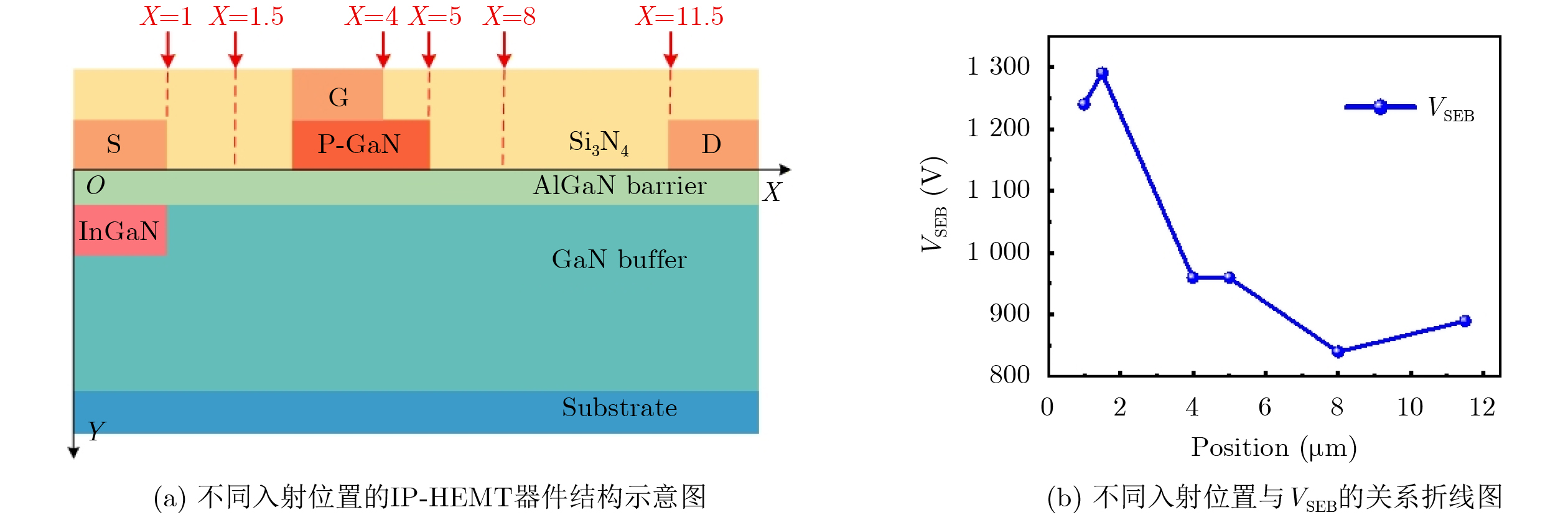
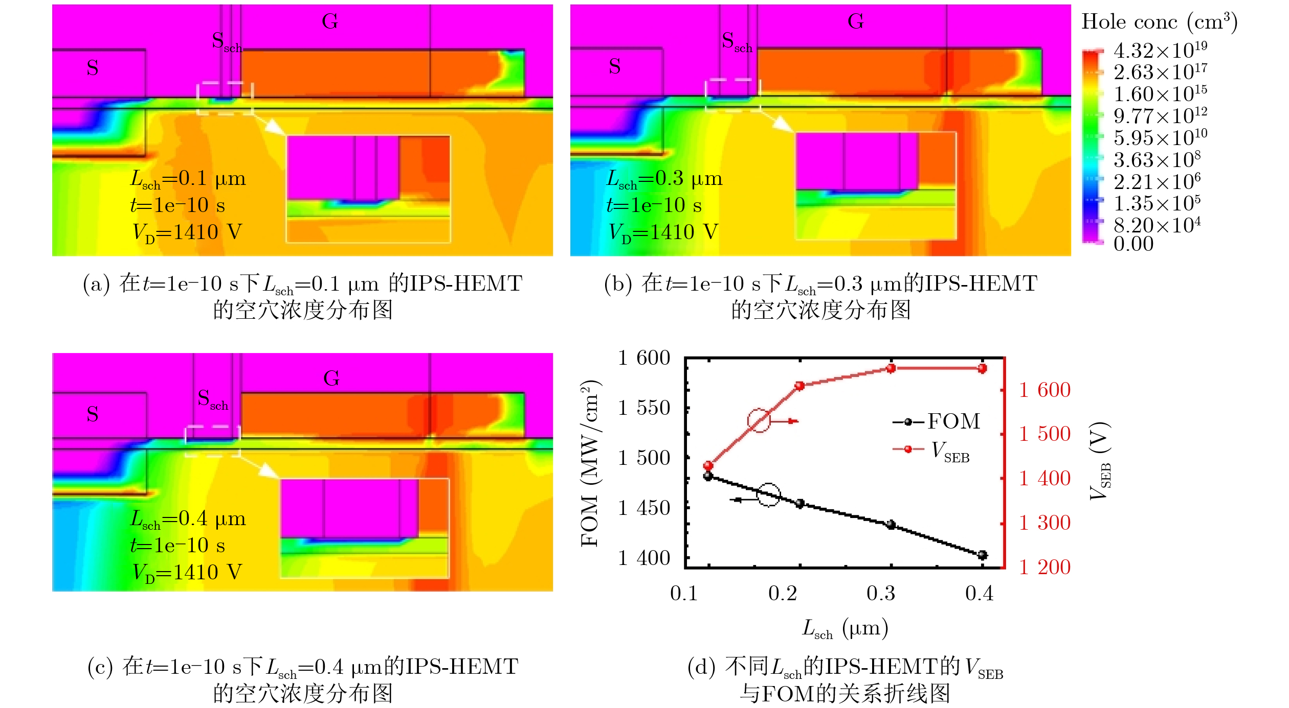
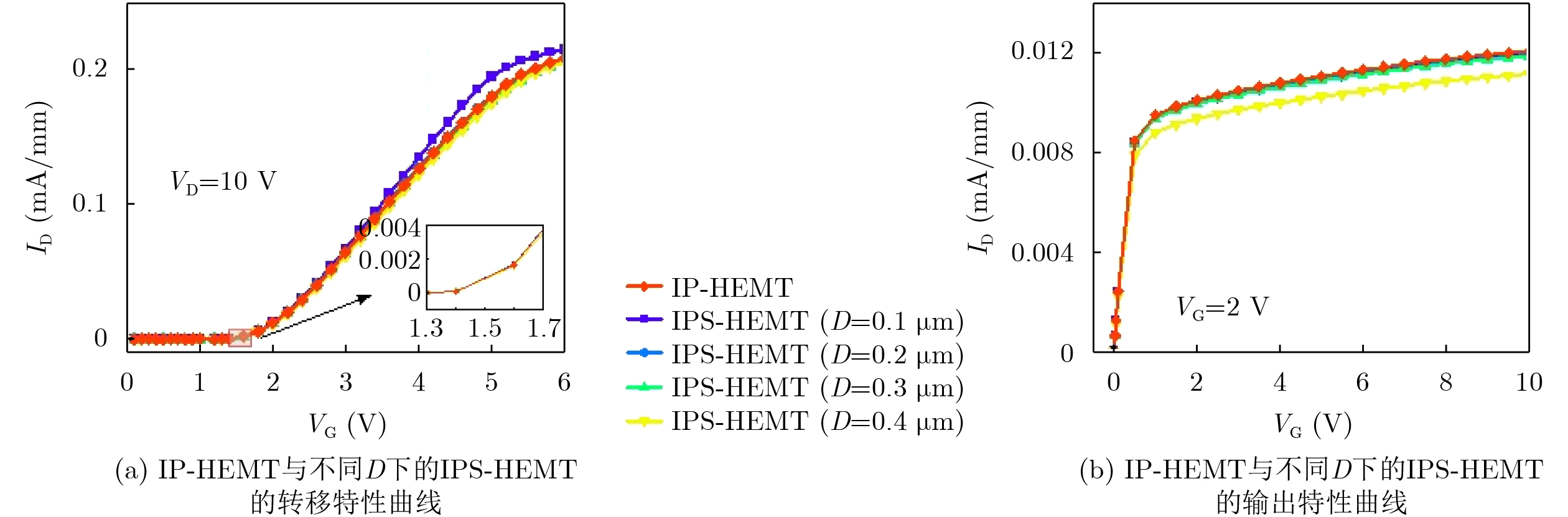
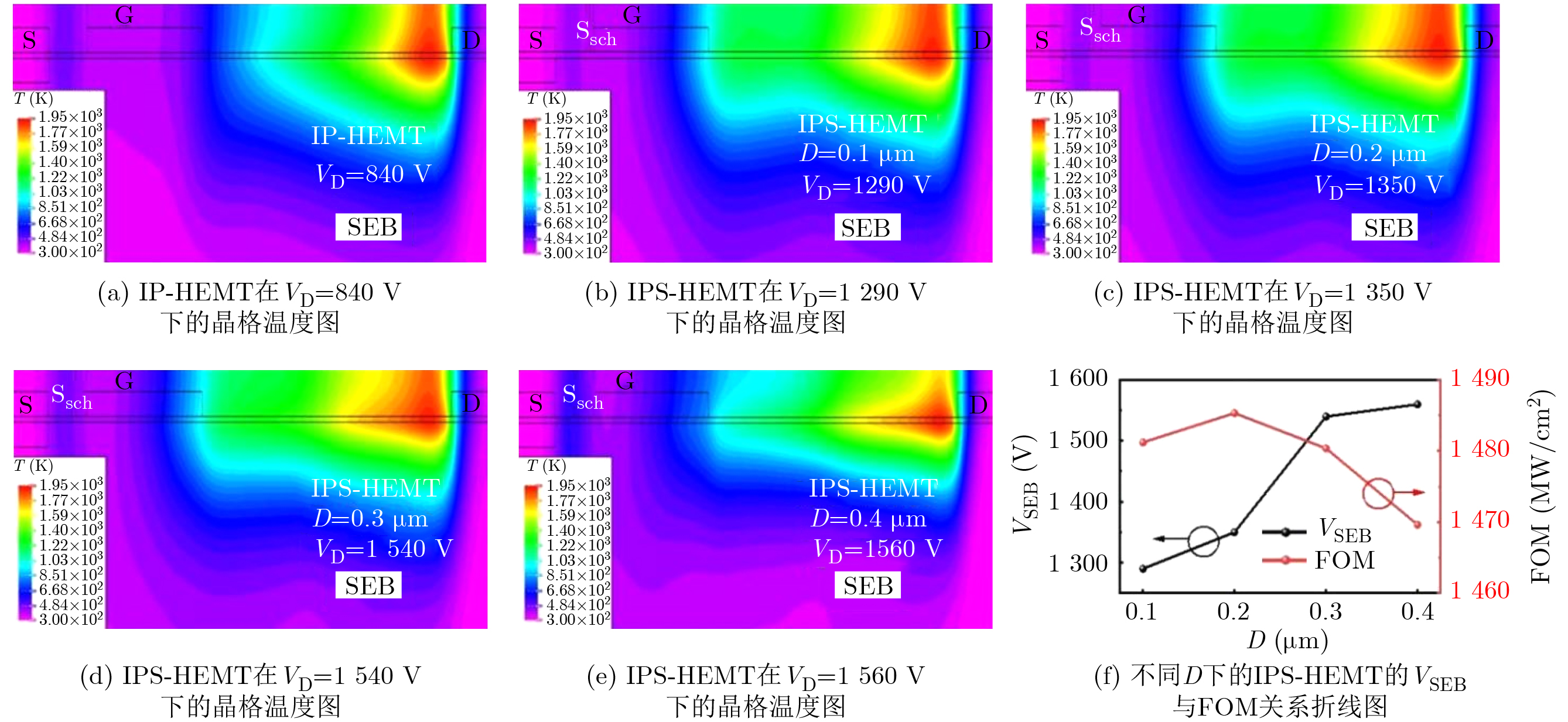
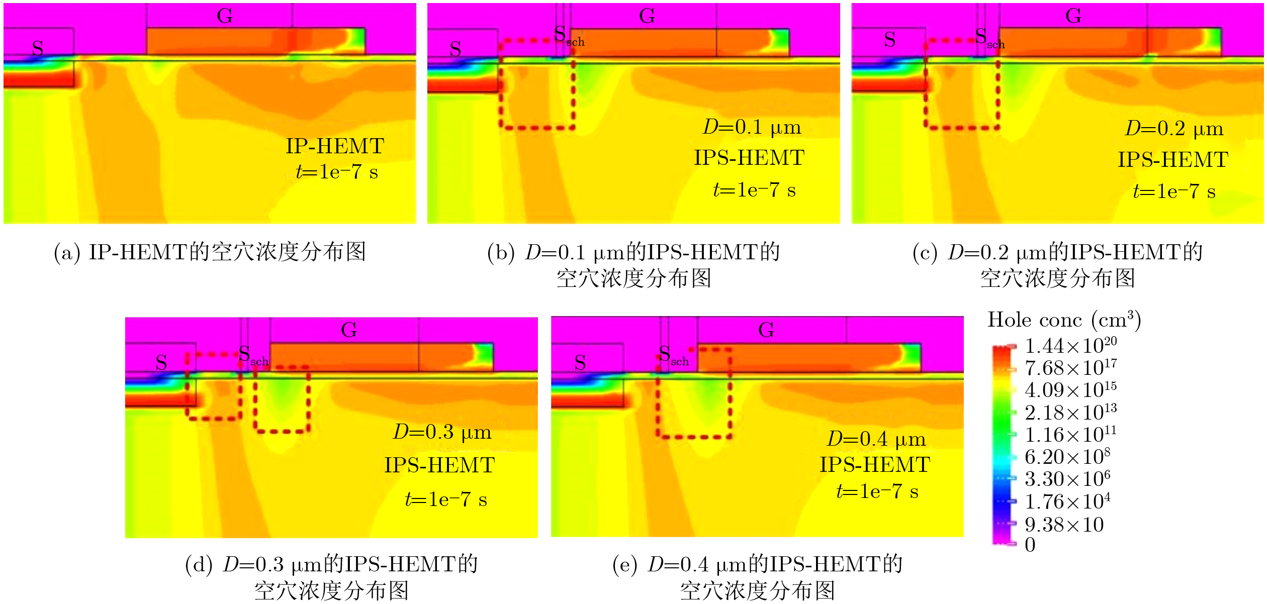
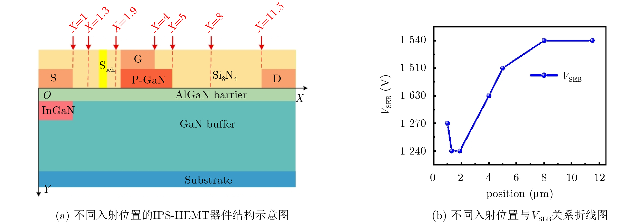
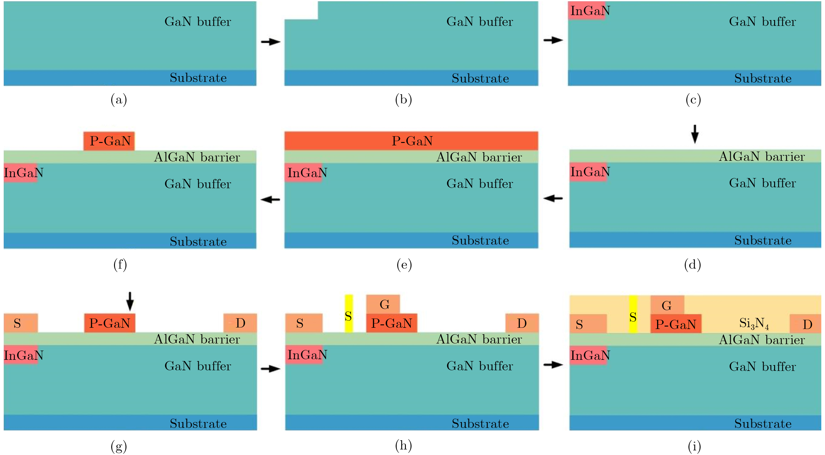
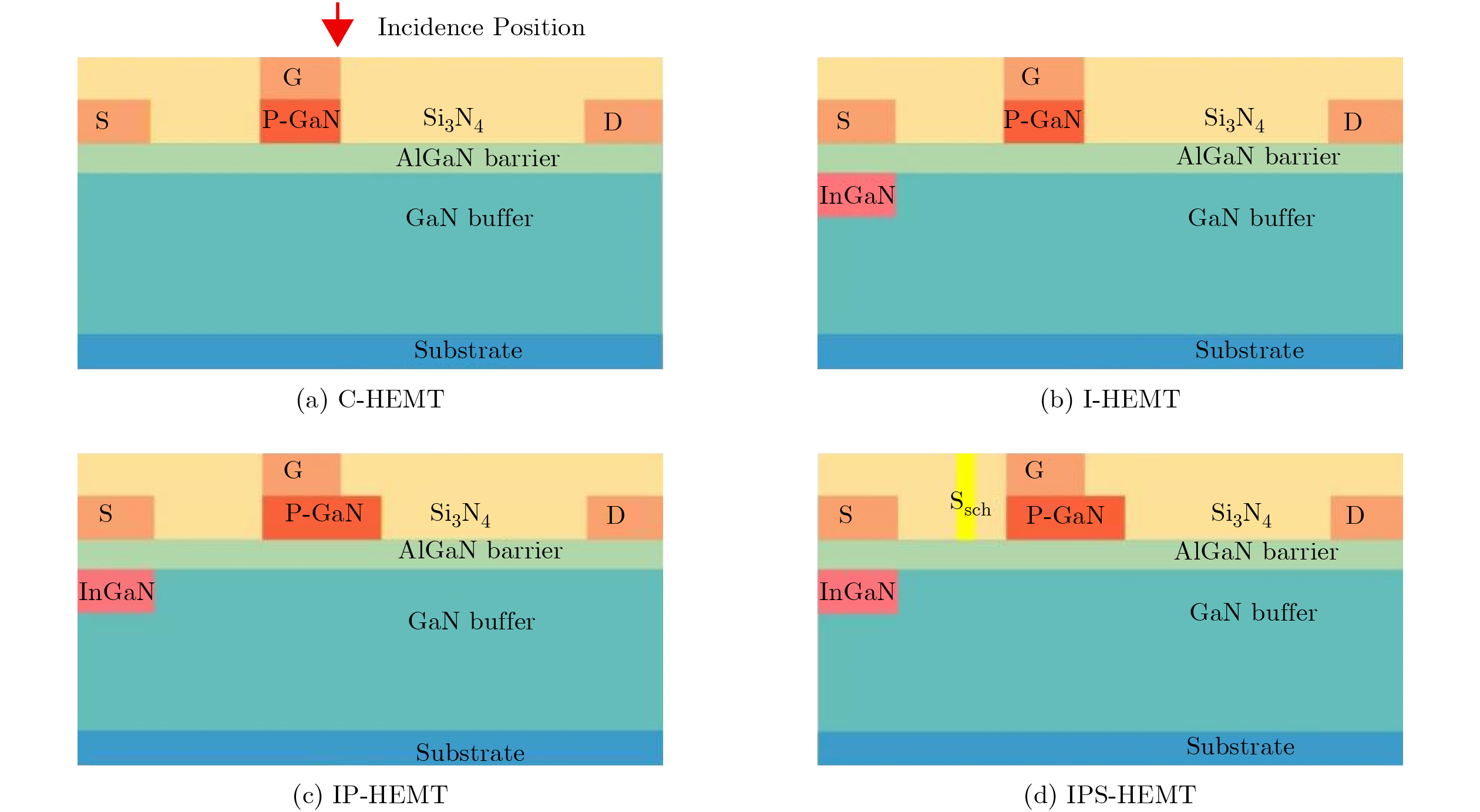
1240 V,增幅327.59%;同时击穿电压(Breakdown Voltage, BV)提升至1765 V,增幅106.4%。该设计通过多重电场调制与载流子耗尽调控机制,实现了抗单粒子烧毁能力与静态特性的良好折中,为宇航级GaN功率器件的辐射加固提供了可行方案。Abstract:Objective A radiation-hardened p-GaN gate HEMT integrating a linearly graded InGaN layer and a Schottky-assisted source (IPS-HEMT) is proposed for improving the tolerance of GaN power devices to heavy-ion-induced single-event burnout (SEB). Heavy-ion irradiation generates a dense electron–hole plasma in the device, and the resulting carrier multiplication, parasitic bipolar conduction, and electrothermal feedback can cause irreversible failure under the off-state high electric field. The proposed structure addresses these processes through three coordinated modifications. A graded InGaN layer is introduced beneath the source, with the indium composition decreasing linearly from 0.8 to 0.2 to generate a polarization-induced two-dimensional hole gas (2DHG) and enhance carrier depletion and recombination. The p-GaN gate is extended toward the drain to reshape the electric-field distribution and suppress carrier accumulation in the gate–drain region. In addition, a Schottky-assisted source is inserted between the gate and the conventional ohmic source to provide an additional path for radiation-induced hole extraction. The effects of the InGaN-layer length, p-GaN extension-layer doping concentration and length, Schottky-source length, and Schottky-source–gate spacing are systematically evaluated. The objective is to identify a structural combination that improves SEB tolerance while retaining acceptable breakdown and on-state characteristics. Methods Two-dimensional TCAD simulations are conducted for a conventional C-HEMT, an I-HEMT containing the graded InGaN layer, an IP-HEMT containing the p-GaN extension layer, and the final IPS-HEMT. The simulations incorporate hydrodynamic carrier transport, field-dependent mobility, high-field mobility saturation, Shockley–Read–Hall and Auger recombination, impact ionization, spontaneous and piezoelectric polarization, and a thermodynamic model. A heavy-ion track is introduced perpendicular to the device surface, and the generated electron–hole pairs are described by spatial and temporal Gaussian distributions. The ion linear energy transfer is set to 63.8 MeV·cm2/mg. Static transfer and output characteristics of the calibrated C-HEMT are first compared with published experimental data to establish the electrical-model baseline ( Fig. 2(a,b) ). The SEB threshold is then determined from the lowest drain bias at which the transient drain current fails to return to the off-state level within the simulated time window. The breakdown voltage, transient current, carrier concentration, lattice temperature, small-signal gate capacitances, and Baliga figure of merit are jointly examined. This procedure separates fixed-position parameter comparisons from the device-level minimum and avoids the use of a single electrical metric to evaluate radiation hardening.Results and Discussions The calibrated C-HEMT reproduces the measured transfer and output characteristics within the compared bias range ( Fig. 2(a-b) ). For each device, VSEB is defined as the minimum SEB threshold obtained from the lateral ion-incidence scan. The C-HEMT exhibits a VSEB of 290 V. Introducing the graded InGaN layer produces a strong length dependence. When the layer length is 0.7–0.9 μm, VSEB increases only to approximately 310 V, whereas a length of 1 μm raises VSEB to 910 V (Fig. 4 ). The corresponding carrier distributions show that the 1 μm layer more effectively depletes the residual channel electrons beneath the source and reduces the electron flux entering the high-field gate–drain region (Fig. 5 ). The 2DHG-related carrier redistribution is also accompanied by lower radiation-induced hole accumulation than in the conventional C-HEMT (Fig. 6 ). Adding the p-GaN extension layer further modifies the off-state carrier distribution and electric field. An acceptor concentration of 4×1018 cm–3 provides the best combined result among the investigated concentrations, with a VSEB of 840 V and an FOM of1290.73 MW/cm2 (Fig. 9 ). Increasing the extension length to 1 μm gives the most favorable FOM–VSEB compromise in the length sweep, while the gate capacitance remains nearly unchanged because the increase in CGS is partly offset by the decrease in CGD (Figs. 10 and11 ). The subsequent Schottky-assisted source supplies an additional hole-collection path. Increasing the Schottky-source length improves VSEB but reduces the FOM, so 0.1 μm is selected for the final structure (Fig. 14 ). For the Schottky-source–gate spacing, 0.3 μm gives the preferred compromise between transient robustness and static performance (Figs. 15 and16 ). Finally, the lateral-incidence scan identifies the most vulnerable positions near the two sides of the Schottky-assisted source, yielding a minimum VSEB of1240 V for the optimized IPS-HEMT (Fig. 18 ).Conclusions A TCAD-based radiation-hardening design is developed by integrating a graded InGaN layer, a p-GaN extension layer, and a Schottky-assisted source into a p-GaN gate HEMT. The results show that the graded InGaN layer is effective only when its length is sufficient to deplete the source-side residual channel and reduce carrier injection into the high-field region. The p-GaN extension then redistributes the electric field and expands the region in which radiation-induced carriers can be controlled. The Schottky-assisted source provides an additional local route for hole extraction, but its geometrical parameters must be optimized because an excessively long source or wide spacing can increase the conduction penalty. The optimized design reaches a device-level VSEB of 1240 V, whereas the conventional C-HEMT exhibits a VSEB of 290 V. The breakdown voltage increases from 855 V to1765 V. These values correspond to improvements of 327.59% and 106.4%, respectively. The simulations also indicate that the total gate capacitance is not substantially increased by the selected p-GaN extension length under the examined small-signal conditions. The improvement is consequently associated with the combined regulation of carrier concentration, electric-field distribution, and hole transport rather than with a single structural component.-
Key words:
- GaN HEMT /
- Single-Event Burnout(SEB) /
- Graded InGaN /
- Schottky source /
- Radiation hardening
-
表 1 IPS-HEMT的主要参数
器件参数 值 InGaN层中铟的摩尔组分 0.2–0.8 InGaN梯度层的长度(LInGaN) 可变 InGaN梯度层的厚度 0.1 μm 肖特基源电极的长度(Lsch) 可变 肖特基辅助源极与栅极之间的距离(D) 可变 p-GaN扩展层的长度(Lp-GaN) 可变 p-GaN扩展层的掺杂浓度(C) 可变  下载: 导出CSV
-
[1] 柏娜, 李钢, 许耀华, 等. 应用于航空航天领域的低功耗多节点抗辐射静态随机存取存储器设计[J]. 电子与信息学报, 2025, 47(3): 850–858. doi: 10.11999/JEIT240294.BAI Na, LI Gang, XU Yaohua, et al. Low-power multi-node radiation-hardened SRAM design for aerospace applications[J]. Journal of Electronics & Information Technology, 2025, 47(3): 850–858. doi: 10.11999/JEIT240294. [2] 闫爱斌, 李坤, 黄正峰, 等. 两种面向宇航应用的高可靠性抗辐射加固技术静态随机存储器单元[J]. 电子与信息学报, 2024, 46(10): 4072–4080. doi: 10.11999/JEIT240082.YAN Aibin, LI Kun, HUANG Zhengfeng, et al. Two highly reliable radiation hardened by design static random access memory cells for aerospace applications[J]. Journal of Electronics & Information Technology, 2024, 46(10): 4072–4080. doi: 10.11999/JEIT240082. [3] 马超, 陈伟中, 张波. 集成肖特基二极管的分裂栅碳化硅(SiC)MOSFET器件[J]. 电子与信息学报, 2025, 47(9): 3346–3352. doi: 10.11999/JEIT250180.MA Chao, CHEN Weizhong, and ZHANG Bo. A novel silicon carbide (SiC) MOSFET with Schottky diode integration technology[J]. Journal of Electronics & Information Technology, 2025, 47(9): 3346–3352. doi: 10.11999/JEIT250180. [4] 高升, 章先锋, 陈秋锐, 等. 集成JFET续流二极管的低开关损耗双沟槽SiC MOSFET[J]. 电子与信息学报, 2025, 47(9): 3303–3311. doi: 10.11999/JEIT250237.GAO Sheng, ZHANG Xianfeng, CHEN Qiurui, et al. Low switching loss double trench SiC MOSFET with integrated JFET continuity diode[J]. Journal of Electronics & Information Technology, 2025, 47(9): 3303–3311. doi: 10.11999/JEIT250237. [5] MISHRA U K, PARIKH P, and WU Yifeng. AlGaN/GaN HEMTs—an overview of device operation and applications[J]. Proceedings of the IEEE, 2002, 90(6): 1022–1031. doi: 10.1109/JPROC.2002.1021567. [6] AMBACHER O, SMART J, SHEALY J R, et al. Two-dimensional electron gases induced by spontaneous and piezoelectric polarization charges in N- and Ga-face AlGaN/GaN heterostructures[J]. Journal of Applied Physics, 1999, 85(6): 3222–3233. doi: 10.1063/1.369664. [7] LV Ling, GUO Changjuan, XING Muhan, et al. Single-event effects of AlGaN/GaN HEMTs under different biases[J]. IEEE Transactions on Electron Devices, 2025, 72(5): 2467–2473. doi: 10.1109/TED.2025.3550111. [8] SEHRA K, CHANCHAL, MALIK A, et al. On the single-event burnout performance of a GaN HEMT with sunken source-connected field plate architecture[J]. IEEE Transactions on Electron Devices, 2024, 71(7): 4072–4078. doi: 10.1109/TED.2024.3396781. [9] SUN Shuxiang, XIE Xintong, ZHANG Pengfei, et al. Improvement of single event transients effect for a novel AlGaN/GaN HEMT with enhanced breakdown voltage[J]. Journal of Science: Advanced Materials and Devices, 2024, 9(2): 100692. doi: 10.1016/j.jsamd.2024.100692. [10] WANG Xiaohu, ZHENG Xuefeng, LIN Danmei, et al. Study on the single-event burnout mechanism of p-GaN gate AlGaN/GaN HEMTs[J]. Applied Physics Letters, 2024, 124(17): 173502. doi: 10.1063/5.0190614. [11] ZHEN Zixin, FENG Chun, WANG Quan, et al. Single event burnout hardening of enhancement mode HEMTs with double field plates[J]. IEEE Transactions on Nuclear Science, 2021, 68(9): 2358–2366. doi: 10.1109/TNS.2021.3102980. [12] HUANG Hao, WANG Ying, HUANG Huolin, et al. A reliable single-event burnout hardening method for p-GaN HEMTs: Using dual-layer buffer structure[J]. IEEE Transactions on Nuclear Science, 2025, 72(11): 3515–3522. doi: 10.1109/TNS.2025.3614665. [13] SUN Yongchang, WANG Ying, CUI Wanzhao, et al. Degradation and failure mechanisms of P-GaN HEMTs in single and complex radiation environments[J]. Nuclear Engineering and Technology, 2026, 58(1): 103902. doi: 10.1016/j.net.2025.103902. [14] LIU Yuan, WANG Ying, and HUANG Hao. Study on single-event radiation effects and hardening techniques in GaN HEMTs[J]. Journal of Computational Electronics, 2025, 24(4): 132. doi: 10.1007/s10825-025-02376-5. [15] ZHANG Ga, ZHAO Shenglei, WANG Zhizhe, et al. TCAD simulation of the effect of buffer layer parameters on single event burn-out in p-GaN gate HEMTs[J]. IEEE Transactions on Electron Devices, 2024, 71(7): 4119–4124. doi: 10.1109/TED.2024.3403085. [16] MANDA M and JACOBSON D. Electron emission from nickel-alloy surfaces in cesium vapor[J]. IEEE Transactions on Plasma Science, 1978, 6(2): 200–211. doi: 10.1109/TPS.1978.4317110. [17] LI Jian, WANG Ying, FEI Xinxing, et al. TCAD analysis of single-event burnout caused by heavy ions for a GaN HEMT[J]. Journal of Computational Electronics, 2025, 24(1): 38. doi: 10.1007/s10825-024-02275-1. [18] WU Wangran, XU Wenting, QU Kai, et al. Comprehensive investigation on different ions of geostationary orbit induced single event burnout in GaN HEMT power devices[J]. Microelectronics Reliability, 2023, 149: 115187. doi: 10.1016/j.microrel.2023.115187. [19] SHUR M S, BYKHOVSKI A D, GASKA R, et al. Accumulation hole layer in p-GaN/AlGaN heterostructures[J]. Applied Physics Letters, 2000, 76(21): 3061–3063. doi: 10.1063/1.126579. [20] BALIGA B J. Power semiconductor device figure of merit for high-frequency applications[J]. IEEE Electron Device Letters, 1989, 10(10): 455–457. doi: 10.1109/55.43098. [21] KHANDELWAL S, CHAUHAN Y S, FJELDLY T A, et al. ASM GaN: Industry standard model for GaN RF and power devices—Part I: DC, CV, and RF model[J]. IEEE Transactions on Electron Devices, 2019, 66(1): 80–86. doi: 10.1109/TED.2018.2867874. -

 下载:

图(19) / 表(1)
计量
- 文章访问数: 16
- HTML全文浏览量: 2
- PDF下载量: 0
- 被引次数: 0
