




Communication Performance and Fault Degradation Analysis of Boundary-interface Configurations in 2.5D Chiplet Systems
-
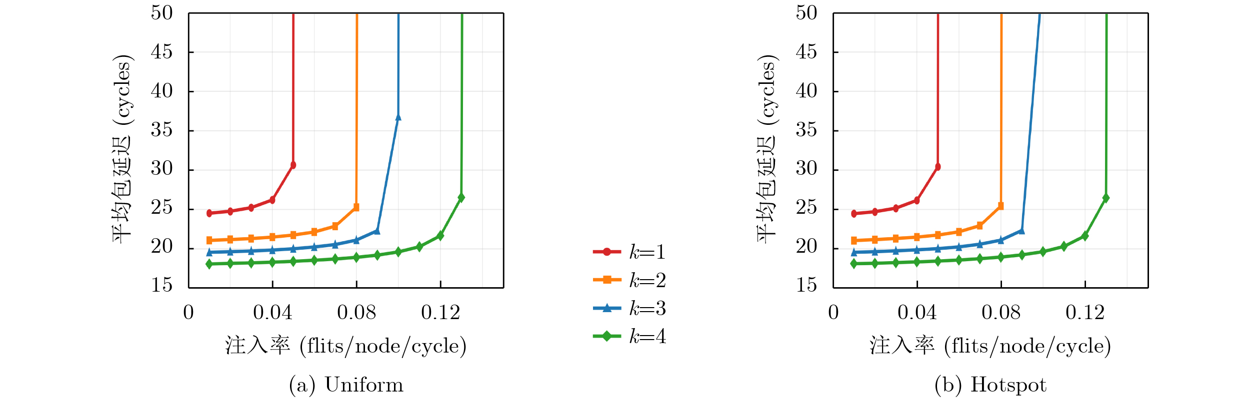
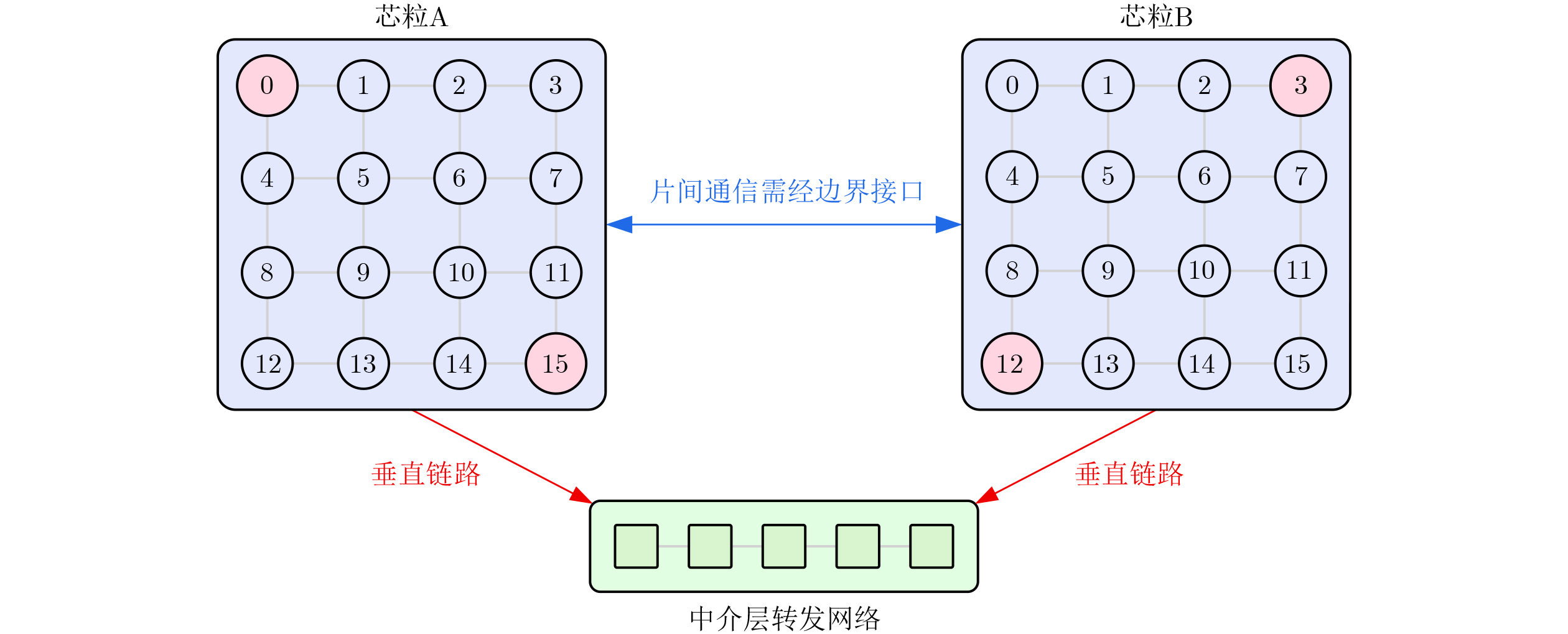
摘要: 受封装资源、微凸点数量和布线约束限制,2.5D芯粒系统的边界接口数量通常有限,并影响片内访问、中介层注入和接口失效后的流量重映射。该文将边界接口配置抽象为片间互连结构参数,建立节点到接口映射和接口服务区域模型,并定义距离、负载均衡和故障退化等图级评价指标。图级分析表明,增加接口数量能够缩短通信距离,但性能收益呈边际递减趋势;相同接口预算下,不同接口位置会诱导不同服务区域并改变接口负载分布;接口失效后,原服务区域向剩余健康接口迁移,主要风险表现为负载再集中。进一步在gem5中构建包含4个内部采用$ 4\times 4 $mesh的芯粒和1个$ 4\times 4 $mesh中介层的网络级周期仿真模型,对代表性布局、接口数量和接口失效进行验证。结果表明,接口数量由$ k=1 $增加到$ k=4 $时,在Uniform和Hotspot流量下,低负载延迟由24.50/24.44 cycle下降到18.05/18.09 cycle,延迟饱和注入率由0.06提高到0.14;在单接口失效遍历下,3种代表性布局的最坏延迟饱和注入率降至0.10~0.11。结果说明,边界接口配置会通过服务区域划分影响访问距离、接口负载和故障重映射,应作为2.5D芯粒片间互连设计中的关键结构参数进行联合评价。Abstract:
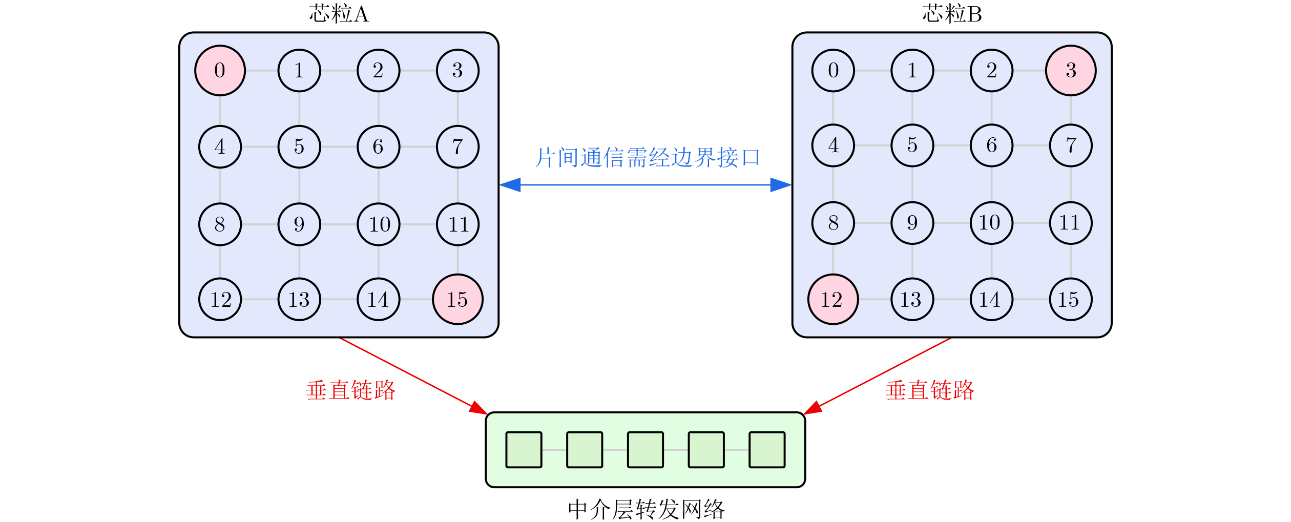
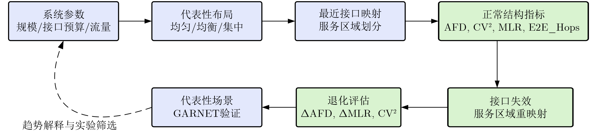
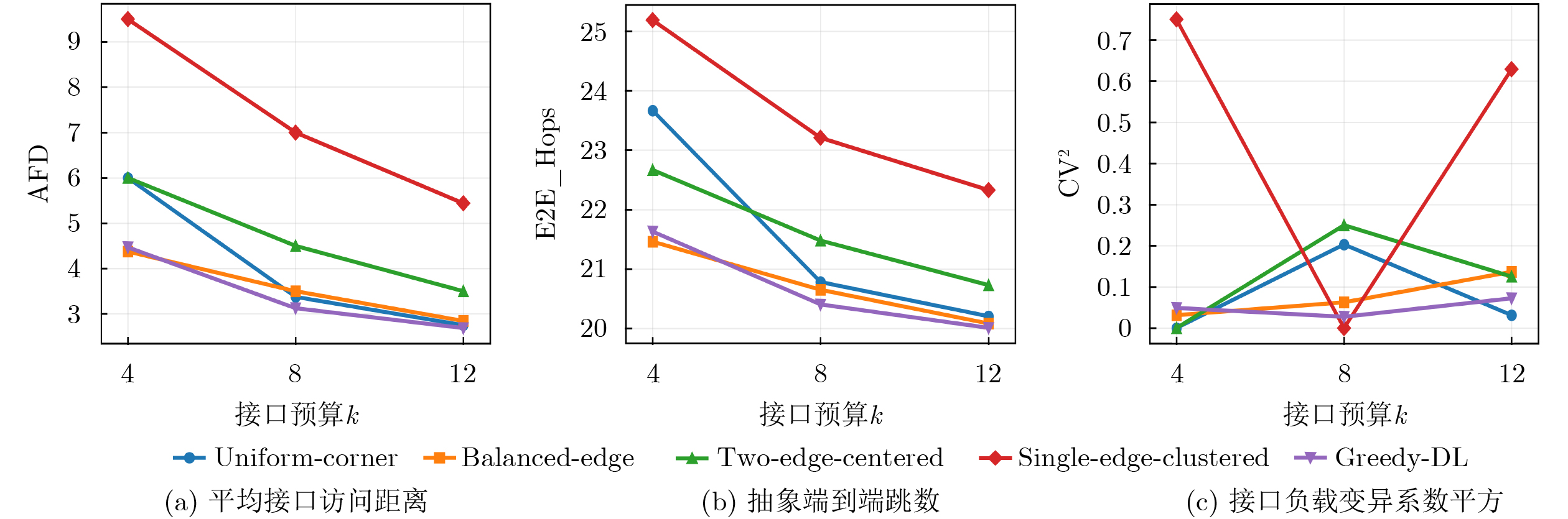
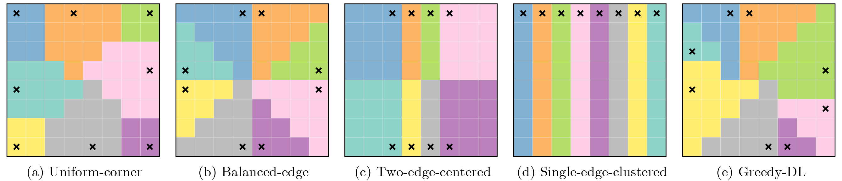
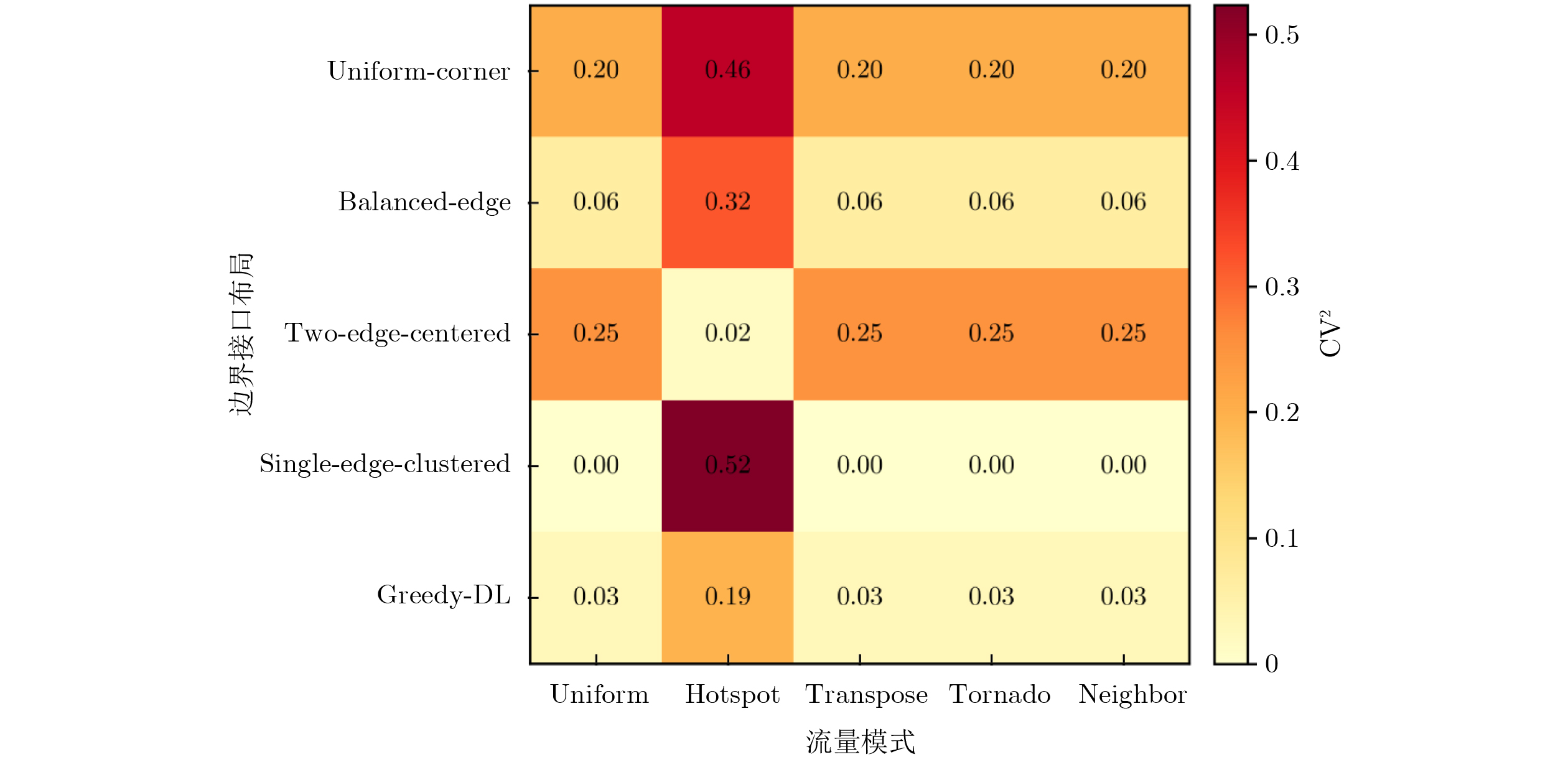
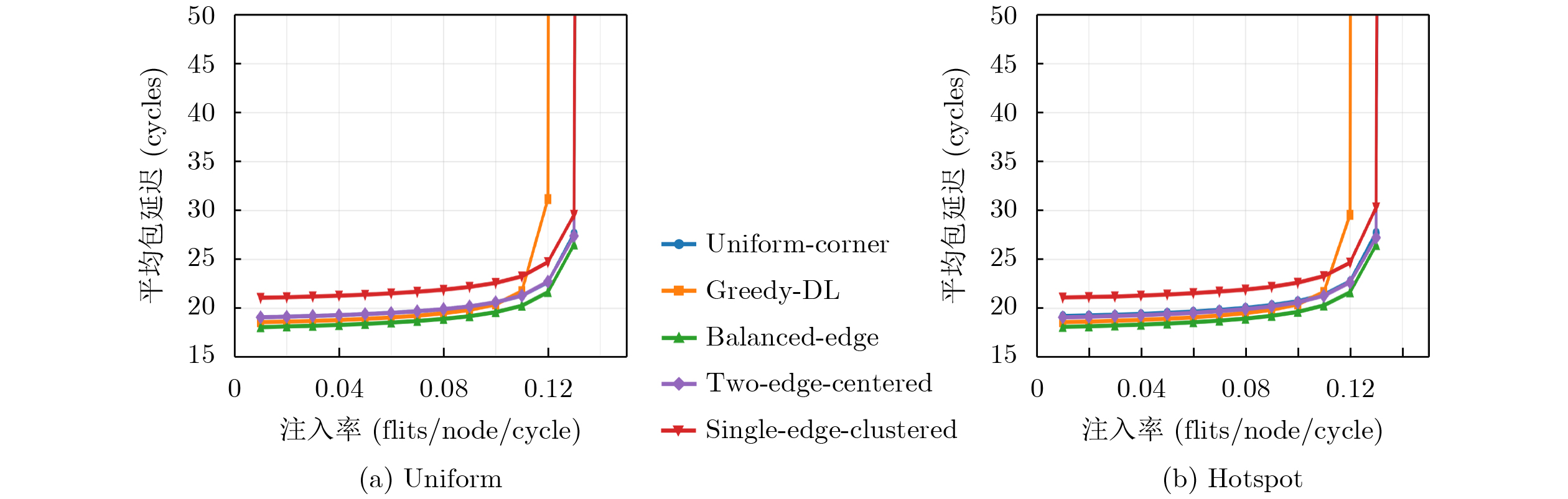
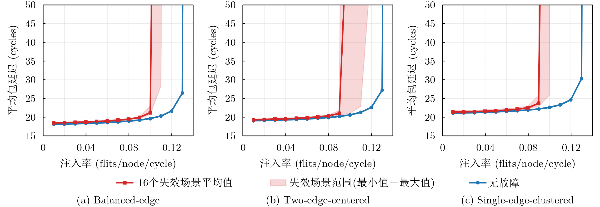
Objective Chiplet-based integration provides an important approach for constructing large-scale heterogeneous systems. In a 2.5D chiplet system, inter-chiplet packets travel from a source node to a boundary interface in the source chiplet, traverse an interposer network, and enter the destination chiplet through a destination-side interface. Because packaging resources, micro-bump count, routing resources, and power and area budgets are limited, interfaces can be deployed only at a subset of boundary nodes. Their number and spatial distribution affect access distance, service-region formation, interface-load distribution, and traffic remapping after failures. Existing studies have addressed die-to-die standards, interposer architectures, placement, routing, simulation, and fault tolerance. However, the independent structural effects of boundary-interface configuration remain insufficiently characterized. This study investigates how interface count, location, service-region partitioning, and failures affect communication performance and fault-induced degradation in 2.5D chiplet–interposer networks. Methods A graph-level structural model is developed for a 2.5D chiplet–interposer network. Each chiplet is modeled as an n × n mesh, and selected boundary nodes serve as active interfaces. Each node is mapped to its nearest active interface, and nodes mapped to the same interface form a service region. Average interface-access distance, abstract end-to-end hop count, squared coefficient of variation of interface load, maximum load ratio, and fault-induced degradation are evaluated. Three chiplet scales, n = 4, 8, and 16, are considered, with corresponding interface budgets of k = 2, 4, 6; k = 4, 8, 12; and k = 8, 16, 24, respectively. Five layouts are analyzed: Uniform-corner, Balanced-edge, Two-edge-centered, Single-edge-clustered, and Greedy-DL. Uniform, Hotspot, Transpose, Tornado, and Neighbor traffic patterns are considered. For fault analysis, each active interface is removed in turn, and affected nodes are remapped to their nearest healthy interfaces. A cycle-accurate gem5 model with Ruby/GARNET, comprising four 4 × 4 mesh chiplets and a 4 × 4 interposer mesh, is constructed. Uniform and Hotspot traffic are evaluated at injection rates from 0.01 to 0.15 flit/node/cycle. The latency saturation injection rate is defined as the first sampled rate at which the average packet latency exceeds 50 cycle. This two-level evaluation separates structural effects from cycle-level network behavior and enables interface count, placement, traffic pattern, and fault location to be compared under consistent topology and routing assumptions. Results and Discussions Graph-level results show that increasing the number of boundary interfaces reduces average interface-access distance and abstract end-to-end hop count, whereas the marginal benefit decreases as boundary coverage becomes sufficient ( Fig. 3 ). Under a fixed interface budget, different interface locations induce different service-region partitions and interface-load distributions (Table 2 ,Fig. 4 ). For an 8 × 8 chiplet with k = 8 under Uniform traffic, Greedy-DL achieves the smallest average interface-access distance of 3.125, whereas Balanced-edge provides a favorable compromise, with an access distance of 3.500 and a maximum load ratio of 1.250. Single-edge-clustered produces the largest access distance and abstract end-to-end hop count because its interfaces are concentrated along one boundary. Under Hotspot traffic, Two-edge-centered reduces the squared coefficient of variation of interface load to 0.016, but its access distance remains higher than those of Balanced-edge and Greedy-DL, indicating a trade-off between distance and load balance (Table 2 ,Fig. 5 ). Interface failures cause only moderate increases in average access distance but substantial load concentration at the remaining healthy interfaces. Under Hotspot traffic, the worst-case maximum-load-ratio degradation is 23.94% for Balanced-edge and 93.75% for both Two-edge-centered and Single-edge-clustered (Table 3 ), indicating that fault sensitivity is mainly associated with service-region migration and load reconcentration. The gem5 results further support the graph-level observations. When the interface count increases from k = 1 to k = 4, low-load latency decreases from 24.50/24.44 cycle to 18.05/18.09 cycle under Uniform and Hotspot traffic, respectively, whereas the latency saturation injection rate increases from 0.06 to 0.14 (Fig. 6 ). Across the k = 4 layouts, Balanced-edge achieves low latency and hop count, whereas Single-edge-clustered has the highest baseline communication cost. Under Hotspot traffic, Balanced-edge reduces low-load latency by about 14.3% and average hop count by about 18.7% compared with Single-edge-clustered. Greedy-DL provides short communication paths under low load, but its latency saturation injection rate is 0.13, lower than the 0.14 achieved by Balanced-edge and several other layouts. This result indicates that minimizing access distance alone does not guarantee better medium- and high-load performance (Fig. 7 ). For fault validation, all 16 single-interface failure scenarios are evaluated for each of the three layouts, yielding 48 scenarios in total. The results show increased latency and hop count, together with an earlier onset of congestion. The worst-case latency saturation injection rate decreases to 0.10~0.11, and Balanced-edge exhibits smaller average and worst-case degradation than the more concentrated layouts (Fig. 8 ,Table 5 ).Conclusions Boundary-interface configuration is a key structural parameter in 2.5D chiplet interconnect design. It affects interface-access distance, service-region formation, interface-load distribution, and fault-induced traffic remapping. Increasing the interface count improves communication efficiency, but the benefit diminishes as boundary coverage increases. Under the same interface budget, interface placement determines whether traffic remains balanced or becomes concentrated after mapping and remapping. The graph-level metrics support low-cost structural screening and mechanism analysis, whereas gem5/Ruby GARNET simulations provide cycle-accurate validation. Therefore, interface count, location, load balance, and fault degradation should be evaluated jointly in 2.5D chiplet–interposer network design. -
Key words:
- Chiplet /
- Interposer network /
- Inter-chiplet interconnect /
- Boundary interface /
- Fault remapping
-
表 1 代表性边界接口布局的主要接口集合
布局 4×4, k=4 8×8, k=8 16×16, k=16 Uniform-corner {0,3,12,15} {0,3,7,31,32,56,60,63} {0,3,7,11,15,63,64,127,128,191,192,240,244,248,252,255} Balanced-edge {1,7,8,14} {3,4,24,31,32,39,59,60} {6,7,8,9,96,111,112,127,128,143,144,159,246,247,248,249} Two-edge-centered {1,2,13,14} {2,3,4,5,58,59,60,61} {4,5,6,7,8,9,10,11,244,245,246,247,248,249,250,251} Single-edge-clustered {0,1,2,3} {0,1,2,3,4,5,6,7} {0,1,2,3,4,5,6,7,8,9,10,11,12,13,14,15} Greedy-DL {1,7,13,14} {3,5,16,31,39,40,59,61} {5,7,8,11,64,95,112,127,128,143,159,176,245,247,250,252} 注:表中集合均为mesh node ID,节点编号及坐标转换规则见第3.1节。  下载: 导出CSV
表 2 $ 8\times 8 $芯粒、$ k=8 $条件下代表性布局的图级结构指标
流量 布局 AFD CV2 MLR E2E_Hops Uniform Uniform-corner 3.375 0.203 1.500 20.781 Uniform Balanced-edge 3.500 0.063 1.250 20.651 Uniform Two-edge-centered 4.500 0.250 1.500 21.479 Uniform Single-edge-clustered 7.000 0.000 1.000 23.208 Uniform Greedy-DL 3.125 0.027 1.250 20.405 Hotspot Uniform-corner 4.472 0.456 1.709 21.795 Hotspot Balanced-edge 4.544 0.317 1.563 21.656 Hotspot Two-edge-centered 5.127 0.016 1.127 22.054 Hotspot Single-edge-clustered 7.000 0.524 2.253 23.034 Hotspot Greedy-DL 4.435 0.192 1.563 21.645
下载: 导出CSV
表 3 $ 8\times 8 $芯粒、$ k=8 $条件下接口失效的图级退化指标(%)
流量 布局 平均$ \Delta \mathrm{AFD} $ 最坏$ \Delta \mathrm{AFD} $ 平均$ \Delta \mathrm{MLR} $ 最坏$ \Delta \mathrm{MLR} $ Hotspot Uniform-corner 1.86 3.00 31.39 56.20 Hotspot Balanced-edge 0.60 0.60 10.41 23.94 Hotspot Two-edge-centered 1.22 1.37 70.75 93.75 Hotspot Single-edge-clustered 0.89 2.01 15.24 93.75 Hotspot Greedy-DL 1.69 2.87 35.16 53.16 Uniform Uniform-corner 2.89 4.17 18.07 21.09 Uniform Balanced-edge 1.34 1.34 35.63 55.00 Uniform Two-edge-centered 1.39 2.08 18.07 29.17 Uniform Single-edge-clustered 0.89 0.89 93.75 93.75 Uniform Greedy-DL 2.56 3.75 25.94 55.00
下载: 导出CSV
表 4 GARNET网络级仿真参数设置
参数 设置 仿真器 gem5 22.1.0.0 with Ruby/GARNET 网络拓扑 4个芯粒,每个芯粒为 $ 4\times 4 $$ 4\times 4 $ mesh;中介层为 $ 4\times 4 $$ 4\times 4 $ mesh 接口数量 $ k=1,2,3,4 $ 接口布局 Uniform-corner, Greedy-DL, Balanced-edge, Two-edge-centered, Single-edge-clustered 流量模式 Uniform random, Hotspot 注入率 0.01~0.15 flits/node/cycle,步长0.01 仿真窗口 100000 cycle;10000 cycle预热周期和90000 cycle统计周期随机性控制 采用gem5默认随机种子;每组配置运行1次 路由策略 片内和中介层均采用确定性维序路由;接口选择采用最近接口映射规则 VNET/VC设置 3个VNET;每个VNET 4个VC;VC缓冲深度4 flits 包长与延迟 1 flit/packet;路由器延迟为1 cycle;链路延迟为1 cycle 统计指标 平均包延迟、平均跳数、延迟-注入率曲线、延迟饱和注入率 延迟饱和注入率 延迟-注入率曲线进入快速增长区间对应的注入率;本文统一采用平均包延迟首次超过50 cycles对应的注入率进行判定
下载: 导出CSV
表 5 Hotspot流量下单接口失效遍历的GARNET网络级退化统计
布局 低负载延迟(cycle)(无故障/
故障平均/故障最坏)平均跳数(无故障/
故障平均/故障最坏)延迟饱和注入率(无故障/
故障平均/故障最坏)Balanced-edge 18.09 / 18.46 / 18.64 6.52 / 6.70 / 6.79 0.14 / 0.1138 / 0.11Two-edge-centered 19.05 / 19.30 / 19.47 7.00 / 7.12 / 7.21 0.14 / 0.1125 / 0.10Single-edge-clustered 21.10 / 21.35 / 21.70 8.02 / 8.14 / 8.32 0.14 / 0.1044 / 0.10
下载: 导出CSV
-
[1] BENINI L and DE MICHELI G. Networks on chips: A new SoC paradigm[J]. Computer, 2002, 35(1): 70–78. doi: 10.1109/2.976921. [2] 邬江兴, 刘勤让, 沈剑良, 等. 从SoC到SDSoW: 微电子发展的新范式[J]. 中国科学: 信息科学, 2024, 54(6): 1350–1368. doi: 10.1360/SSI-2023-0219.WU Jiangxing, LIU Qinrang, SHEN Jianliang, et al. From SoC to SDSoW: A new paradigm for microelectronics development[J]. Scientia Sinica Informationis, 2024, 54(6): 1350–1368. doi: 10.1360/SSI-2023-0219. [3] LIU Yafei, LI Xiangyu, and YIN Shouyi. Review of chiplet-based design: System architecture and interconnection[J]. Science China Information Sciences, 2024, 67(10): 200401. doi: 10.1007/s11432-023-3926-8. [4] 王浩, 王勇, 冯长磊, 等. 芯粒互联技术综述[J]. 计算机研究与发展, 2025, 62(11): 2651–2662. doi: 10.7544/issn1000-1239.202440585.WANG Hao, WANG Yong, FENG Changlei, et al. Review of chiplet interconnection technology[J]. Journal of Computer Research and Development, 2025, 62(11): 2651–2662. doi: 10.7544/issn1000-1239.202440585. [5] ONUFRYK P and CHOUDHARY S. UCIe: Standard for an open chiplet ecosystem[J]. IEEE Micro, 2025, 45(1): 16–25. doi: 10.1109/MM.2024.3451532. [6] NAFFZIGER S, BECK N, BURD T, et al. Pioneering chiplet technology and design for the AMD EPYC™ and Ryzen™ processor families: Industrial product[C]. The 2021 ACM/IEEE 48th Annual International Symposium on Computer Architecture, Valencia, Spain, 2021: 57–70. doi: 10.1109/ISCA52012.2021.00014. [7] KANNAN A, ENRIGHT JERGER N, and LOH G H. Enabling interposer-based disintegration of multi-core processors[C]. The 48th International Symposium on Microarchitecture, Waikiki, USA, 2015: 546–558. doi: 10.1145/2830772.2830808. [8] ENRIGHT JERGER N, KANNAN A, LI Zimo, et al. NoC architectures for silicon interposer systems: Why pay for more wires when you can get them (from your interposer) for free?[C]. The 2014 47th Annual IEEE/ACM International Symposium on Microarchitecture, Cambridge, UK, 2014: 458–470. doi: 10.1109/MICRO.2014.61. [9] LI Fuping, WANG Ying, CHENG Yuanqing, et al. GIA: A reusable general interposer architecture for agile chiplet integration[C]. The 41st IEEE/ACM International Conference on Computer-Aided Design, San Diego, USA, 2022: 42. doi: 10.1145/3508352.3549464. [10] JIAO Bo, XU Lei, YU Xinyu, et al. FPIA: Communication-aware multi-chiplet integration with field-programmable interconnect fabric on reusable silicon interposer[J]. IEEE Transactions on Circuits and Systems I: Regular Papers, 2024, 71(9): 4156–4168. doi: 10.1109/TCSI.2024.3419579. [11] 卢美璇, 许浩博, 王颖, 等. 芯粒集成芯片架构-封装协同设计[J]. 电子与信息学报, 2025, 47(9): 2994–3009. doi: 10.11999/JEIT250626.LU Meixuan, XU Haobo, WANG Ying, et al. Co-design of architecture and packaging in chiplet[J]. Journal of Electronics & Information Technology, 2025, 47(9): 2994–3009. doi: 10.11999/JEIT250626. [12] COSKUN A, ERIS F, JOSHI A, et al. Cross-layer co-optimization of network design and chiplet placement in 2.5-D systems[J]. IEEE Transactions on Computer-Aided Design of Integrated Circuits and Systems, 2020, 39(12): 5183–5196. doi: 10.1109/TCAD.2020.2970019. [13] ZHANG Jinming, FAN Xi, YE Yaoyao, et al. INDM: Chiplet-based interconnect network and dataflow mapping for DNN accelerators[J]. IEEE Transactions on Computer-Aided Design of Integrated Circuits and Systems, 2024, 43(4): 1107–1120. doi: 10.1109/TCAD.2023.3332832. [14] FENG Yinxiao, WEI Yuchen, XIANG Dong, et al. Evaluating chiplet-based large-scale interconnection networks via cycle-accurate packet-parallel simulation[C]. 2024 USENIX Annual Technical Conference (USENIX ATC 24), Santa Clara, USA, 2024: 45. [15] 张聪武, 刘澳, 张科, 等. 面向通用处理器芯粒架构探索和评估的系统级模拟器[J]. 电子与信息学报, 2024, 46(12): 4575–4588. doi: 10.11999/JEIT240299.ZHANG Congwu, LIU Ao, ZHANG Ke, et al. A system-level exploration and evaluation simulator for chiplet-based CPU[J]. Journal of Electronics & Information Technology, 2024, 46(12): 4575–4588. doi: 10.11999/JEIT240299. [16] WANG Xiaohang, XU Miao, SINGH A K, et al. On optimizing inter- and intra-chiplet interconnection topologies for robust multi-chiplet systems[J]. IEEE Transactions on Computer-Aided Design of Integrated Circuits and Systems, 2025, 44(10): 3976–3989. doi: 10.1109/TCAD.2025.3550432. [17] 周武, 倪天明, 徐冬雨, 等. 面向芯粒互连网络的故障与拥塞联合感知自适应路由算法[J]. 电子与信息学报, 2025, 47(9): 3155–3166. doi: 10.11999/JEIT250294.ZHOU Wu, NI Tianming, XU Dongyu, et al. A joint fault and congestion-aware adaptive routing algorithm for chiplet interconnect networks[J]. Journal of Electronics & Information Technology, 2025, 47(9): 3155–3166. doi: 10.11999/JEIT250294. [18] JIANG Nan, BECKER D U, MICHELOGIANNAKIS G, et al. A detailed and flexible cycle-accurate Network-on-Chip simulator[C]. 2013 IEEE International Symposium on Performance Analysis of Systems and Software, Austin, USA, 2013: 86–96. doi: 10.1109/ISPASS.2013.6557149. [19] AGARWAL N, KRISHNA T, PEH L S, et al. GARNET: A detailed on-chip network model inside a full-system simulator[C]. 2009 IEEE International Symposium on Performance Analysis of Systems and Software, Boston, USA, 2009: 33–42. doi: 10.1109/ISPASS.2009.4919636. [20] BINKERT N, BECKMANN B, BLACK G, et al. The gem5 simulator[J]. ACM SIGARCH Computer Architecture News, 2011, 39(2): 1–7. doi: 10.1145/2024716.2024718. [21] MAHMUD T and WANG Ke. A flexible hybrid interconnection design for high-performance and energy-efficient chiplet-based systems[J]. IEEE Computer Architecture Letters, 2024, 23(2): 215–218. doi: 10.1109/LCA.2024.3477253. [22] TAHERI E, PASRICHA S, and NIKDAST M. DeFT: A deadlock-free and fault-tolerant routing algorithm for 2.5D chiplet networks[C]. 2022 Design, Automation & Test in Europe Conference & Exhibition, Antwerp, Belgium, 2022: 1047–1052. doi: 10.23919/DATE54114.2022.9774617. [23] EHRETT P, AUSTIN T, and BERTACCO V. SiPterposer: A fault-tolerant substrate for flexible system-in-package design[C]. 2019 Design, Automation & Test in Europe Conference & Exhibition, Florence, Italy, 2019: 510–515. doi: 10.23919/DATE.2019.8714998. [24] MARINISSEN E J, EVANS A, CHUANG P Y, et al. New standard-under-development for chiplet interconnect test and repair: IEEE Std P3405[C]. 2024 IEEE European Test Symposium, The Hague, Netherlands, 2024: 1–10. doi: 10.1109/ETS61313.2024.10567355. [25] BHOUMIK P, CHAUDHURI A, GOEL S K, et al. Fault modeling and testing of chiplet-to-chiplet interconnects in fan-out wafer-level packaging[C]. 2025 IEEE International Test Conference, San Diego, USA, 2025: 357–366. doi: 10.1109/ITC58126.2025.00043. [26] 王知非, 黄之闻, 叶天辰, 等. 面向芯粒互连的单端64 Gb/s全双工收发机设计[J]. 电子与信息学报, 2025, 47(9): 2979–2993. doi: 10.11999/JEIT250506.WANG Zhifei, HUANG Zhiwen, YE Tianchen, et al. A 64 Gb/s single-ended simultaneous bi-directional transceiver for die-to-die interfaces[J]. Journal of Electronics & Information Technology, 2025, 47(9): 2979–2993. doi: 10.11999/JEIT250506. -

 下载:
下载:

图(8) / 表(5)
计量
- 文章访问数: 354
- HTML全文浏览量: 107
- PDF下载量: 37
- 被引次数: 0
