




Design of a Low-Cost High-Isolation RF Switch for X-Band Active Phased Array T/R Modules
-
摘要: 针对低成本PIN二极管在X波段因寄生参数、接地通孔寄生效应导致开关隔离度降低与插入损耗增加的问题,该文提出一种基于寄生参数补偿的X波段低成本高隔离度并联型射频开关电路设计方法。所提方法通过引入补偿短截线与T型结等效结构电容,分别抵消不同工作状态下的寄生电抗,解决了低成本器件的高频性能恶化问题。实测结果表明,该射频开关电路在9.5~10.4 GHz频段内回波损耗优于10 dB,隔离度高于20 dB,插入损耗低于2 dB。该设计具有结构简单、易于集成、成本较低等优势,验证了低成本二极管用于X波段高隔离度T/R组件射频开关的可行性。
-
关键词:
- 有源相控阵 /
- T/R组件 /
- 高隔离度射频开关电路 /
- 寄生参数补偿
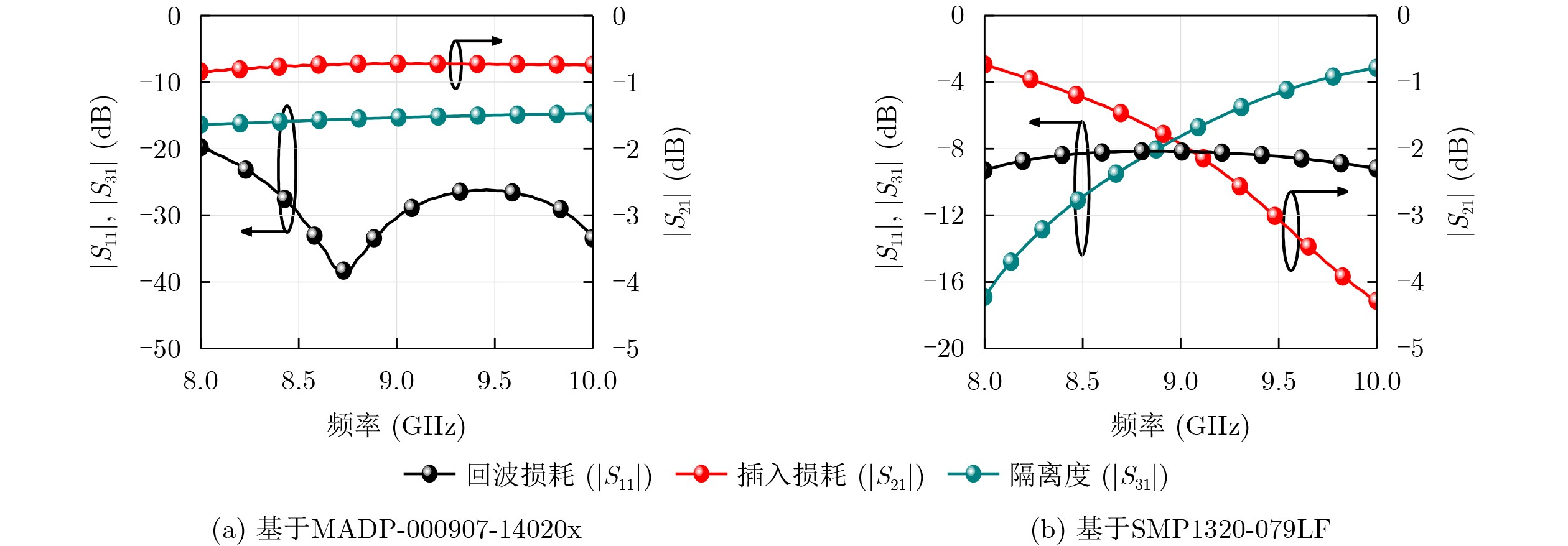
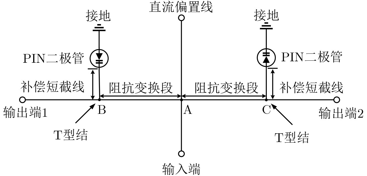
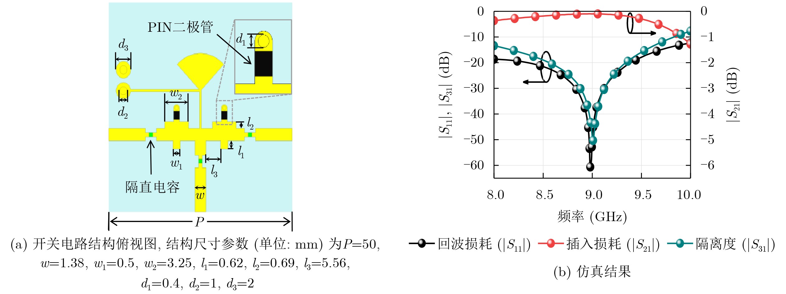
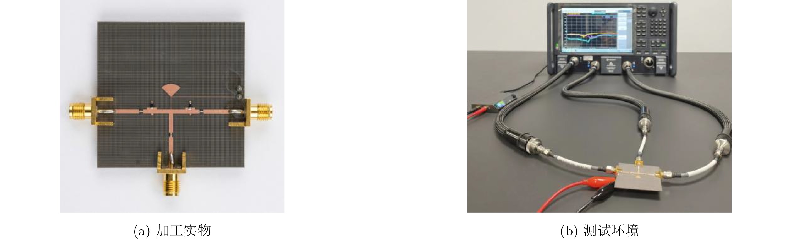
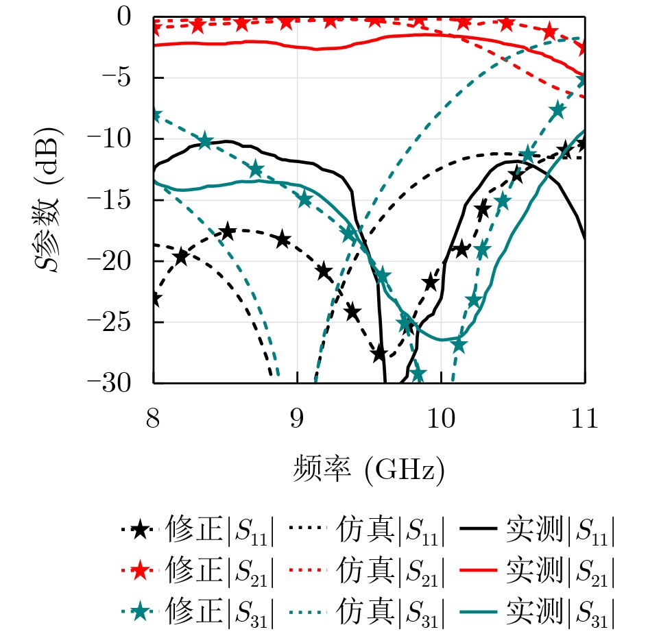
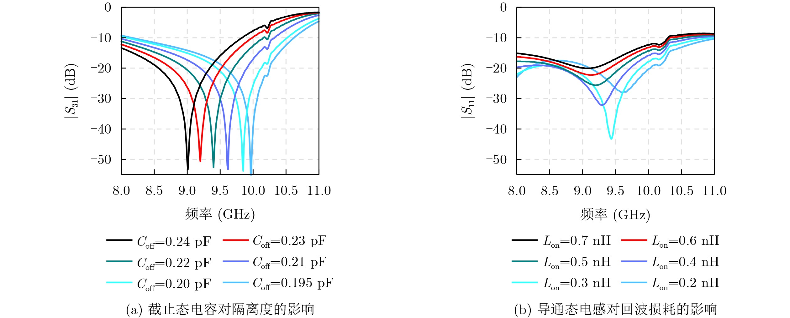
Abstract:Objective Radio frequency (RF) switches are key front-end components in communication and radar systems, especially in active phased array transmit/receive (T/R) modules. Positive-intrinsic-negative (PIN) diodes are widely used in high-power microwave switches because of their high power-handling capability, good linearity, and mature fabrication process. However, low-cost plastic-packaged PIN diodes exhibit significant parasitic effects at X-band frequencies. Junction capacitance, package inductance, and grounding-via inductance cause shunt branches to deviate from ideal short- or open-circuit conditions, resulting in degraded isolation and increased insertion loss. To address this problem, a low-cost high-isolation X-band single-pole double-throw (SPDT) RF switch design method based on parasitic-parameter compensation is proposed. Methods A step-wise synergistic matching strategy, termed “OFF-state prioritized determination and ON-state structural compensation”, is developed. OFF-state isolation and ON-state transmission conditions are treated separately to reduce coupling between isolation and transmission objectives. For the isolation branch, OFF-state diode parasitic parameters, a compensation stub, and grounding-via inductance are combined to form a series-resonant network. By compensating parasitic reactance, the branch satisfies the required impedance condition and suppresses signal leakage. After the compensation-stub parameters are determined, ON-state compensation is realized by introducing equivalent structural capacitance through T-junction edge effects and a stepped-impedance main line. This capacitance, together with the total equivalent inductance of the shunt branch, forms a parallel-resonant network, making the branch approach an open-circuit condition at the operating frequency. Thus, signal shunting is reduced and low-insertion-loss transmission is achieved without additional lumped compensation components. Results and Discussions The proposed switch topology is presented, and a full-wave simulation model is established ( Fig. 3 ,Fig. 4(a) ). Simulation results show that return loss is better than 20 dB, isolation is higher than 20 dB, and insertion loss remains around 0.2 dB over 8.57–9.34 GHz (Fig. 4(b) ). A prototype is fabricated and measured (Fig. 5 ). Measurement results show that, over 9.5–10.4 GHz, return loss is better than 10 dB, insertion loss is lower than 2 dB, and isolation is higher than 20 dB (Fig. 6 ). Although the measured operating band shifts upward by about 1 GHz relative to initial simulation results, measured trends remain consistent with theoretical analysis. To explain this frequency shift, OFF-state junction capacitance and ON-state parasitic inductance are further analyzed. As OFF-state junction capacitance decreases from 0.24 pF to 0.195 pF, the high-isolation band shifts to higher frequencies (Fig. 7 (a)). With OFF-state capacitance fixed at 0.195 pF, reducing ON-state parasitic inductance from 0.7 nH to 0.2 nH shifts the return-loss response to higher frequencies (Fig. 7(b) ). After parameter correction, simulated return loss, insertion loss, and isolation agree more closely with measured results (Fig. 6 ). Compared with existing SPDT RF switch designs, the proposed design uses low-cost plastic-packaged PIN diodes and a simple microstrip compensation structure, requires no additional lumped compensation components, reduces dependence on the high intrinsic OFF-state impedance of PIN diodes, and achieves a good balance between cost and high-frequency switch performance (Table 1 ).Conclusions A low-cost high-isolation X-band SPDT RF switch based on parasitic-parameter compensation is presented. By using OFF-state series resonance and ON-state structural capacitance compensation, high isolation and low insertion loss are realized simultaneously. The fabricated switch achieves isolation higher than 20 dB and insertion loss lower than 2 dB over 9.5-10.4 GHz. The switch features a simple structure, ease of integration, and low cost, and provides a practical reference for low-cost high-isolation T/R module RF switches in active phased array systems. -
表 1 本文工作与现有SPDT射频开关方案的性能对比
文献 器件与技术路线 工作频率(GHz) 插入损耗(dB) 回波损耗(dB) 隔离度(dB) 成本 高阻抗依赖 [9] GaAs pHEMT晶体管+
电容加载堆叠FET结构DC–40 <3 >11 >39 高 未涉及 [10] 塑封PIN二极管+
集总RLC补偿与匹配网络1.02–3.36 <0.81 >20 >27 中 是 [11] GaAs PIN二极管+
多管串联结构37.7–61 <1.5 >10 >24.6 高 是 [12] CMOS晶体管+
差分结构与泄漏抵消电容24–40 <1.6 >10 >30 高 未涉及 本文 塑封PIN二极管+
微带结构补偿9.5–10.4 <2 >10 >20 低 否  下载: 导出CSV
-
[1] HAIDER J, KHAN W, NADEEM A, et al. Design of a compact T/R module for an all-digital S-band phased array radar system[C]. 2025 2nd International Conference on Microwave, Antennas & Circuits (ICMAC), Islamabad, Pakistan, 2025: 1–4. doi: 10.1109/ICMAC64768.2025.11003263. [2] SHAO Bingqian, LU Chengjian, XIANG Yinjie, et al. Comprehensive review of RF MEMS switches in satellite communications[J]. Sensors, 2024, 24(10): 3135. doi: 10.3390/s24103135. [3] YOU Changsheng, CAI Yunlong, LIU Yuanwei, et al. Next generation advanced transceiver technologies for 6G and beyond[J]. IEEE Journal on Selected Areas in Communications, 2025, 43(3): 582–627. doi: 10.1109/JSAC.2025.3536557. [4] REBEIZ G M and MULDAVIN J B. RF MEMS switches and switch circuits[J]. IEEE Microwave Magazine, 2001, 2(4): 59–71. doi: 10.1109/6668.969936. [5] KURMENDRA and AGARWAL S. MEMS switch realities: Addressing challenges and pioneering solutions[J]. Micromachines, 2024, 15(5): 556. doi: 10.3390/mi15050556. [6] TAIT R N. Progress in RF-MEMS[J]. Micromachines, 2025, 16(2): 233. doi: 10.3390/mi16020233. [7] LI Qiqi, LENG Yongqing, QIU Xin, et al. A 6–18 GHz high power-handling switch in GaN technology[C]. 2023 IEEE MTT-S International Microwave Workshop Series on Advanced Materials and Processes for RF and THz Applications (IMWS-AMP), Chengdu, China, 2023: 1–3. doi: 10.1109/IMWS-AMP57814.2023.10381466. [8] HUANG C T, LIN Y S, HUANG C Y, et al. Design and analysis of SPDT switch and array antenna for 28 GHz 5G new radio[C]. 2024 IEEE/MTT-S International Microwave Symposium - IMS 2024, Washington, USA, 2024: 757–759. doi: 10.1109/IMS40175.2024.10600305. [9] TSAO C M and HSU H T. An ultra-wideband, high power and high isolation single-pole-double-throw switch using capacitive loading approach[J]. IEEE Transactions on Circuits and Systems II: Express Briefs, 2023, 70(11): 4013–4017. doi: 10.1109/TCSII.2023.3286884. [10] ZHOU Pinhao, SHEN Guangxu, FENG Wenjie, et al. A compact wideband SPDT switch using compensating inductors and highpass matching network[J]. IEEE Transactions on Circuits and Systems I: Regular Papers, 2025, 72(8): 3961–3970. doi: 10.1109/TCSI.2024.3479424. [11] HSIEH Y C, LIN G J, TSAI Z M, et al. A Q-/V-band 37.6-dBm IP0.1 dB and low loss SPDT switch using three-series PIN diodes connection[J]. International Journal of Microwave and Wireless Technologies, 2025, 17(4): 731–739. doi: 10.1017/S175907872510175X. [12] PARK J, LEE S, and HONG S. A 24–40 GHz differential SPDT switch with an NMOS and PMOS alternating structure and leakage-canceling capacitors[J]. IEEE Transactions on Circuits and Systems II: Express Briefs, 2023, 70(1): 86–90. doi: 10.1109/TCSII.2022.3205907. [13] FORBES T, SAUGEN J, and MAGSTADT B. Differential cancellation based RF switch enabling high isolation and minimal insertion loss in 0.0006 mm2 area[C]. 2022 IEEE Texas Symposium on Wireless and Microwave Circuits and Systems (WMCS), Waco, USA, 2022: 1–4. doi: 10.1109/WMCS55582.2022.9866179. [14] GHORBANI F, ZHOU Jiafeng, HUANG Yi, et al. Impedance-oriented approach for maximizing linearity in p-i-n-diode-based phase shifters[J]. IEEE Transactions on Microwave Theory and Techniques, 2025, 73(8): 4513–4522. doi: 10.1109/TMTT.2025.3547970. [15] LIU Mingming, JIN Ronghong, GENG Junping, et al. Low-insertion loss PIN diode switches using impedance-transformation networks[J]. Progress in Electromagnetics Research C, 2013, 34: 195–202. doi: 10.2528/PIERC12092604. [16] VASSILEV V, VILENSKIY A, CHOU H T, et al. A 55-105 GHz PIN diode SPDT switch[C]. 2021 International Symposium on Antennas and Propagation (ISAP), Taipei, China, 2021: 1–2. doi: 10.23919/ISAP47258.2021.9614359. [17] SINGH A and MANDAL M K. Parasitic compensation and hence isolation improvement of PIN diode-based switches[J]. IEEE Transactions on Circuits and Systems II: Express Briefs, 2021, 68(1): 97–101. doi: 10.1109/TCSII.2020.3000587. [18] ZHANG Yi, ZHOU Yingjie, LU Xinmin, et al. X-band high isolation single pole double throw switch based on resonant concept[J]. Microwave and Optical Technology Letters, 2024, 66(6): e34221. doi: 10.1002/mop.34221. [19] MOON S, KWON J, LEE J, et al. X-band asymmetric GaN HEMT SPDT switch using LC resonator and quarter-wave stub for high power handling capability and high isolation[C]. 2025 20th European Microwave Integrated Circuits Conference (EuMIC), Utrecht, Netherlands, 2025: 339–342. doi: 10.23919/EuMIC65284.2025.11234504. [20] POZAR D M. Microwave Engineering[M]. 4th ed. Hoboken: John Wiley & Sons, 2011: 56–74, 272–277. (查阅网上资料, 未找到本条文献出版地信息, 请确认). [21] GUPTA K C, GARG R, BAHL I, et al. Microstrip Lines and Slotlines[M]. 2nd ed. Boston: Artech House, 1996: 189–208. -


 下载:
下载:


图(7) / 表(1)
计量
- 文章访问数: 16
- HTML全文浏览量: 2
- PDF下载量: 0
- 被引次数: 0
