

Design of Low-Power On-Chip Cache for Visual Perception Systems on the Edge
-
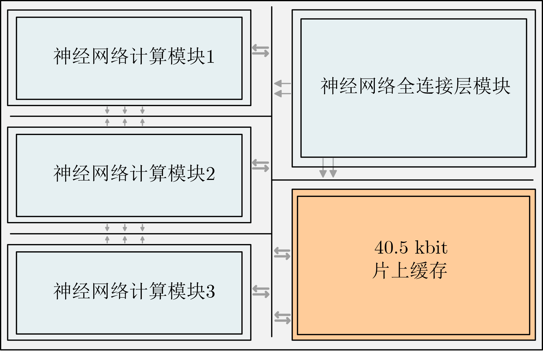
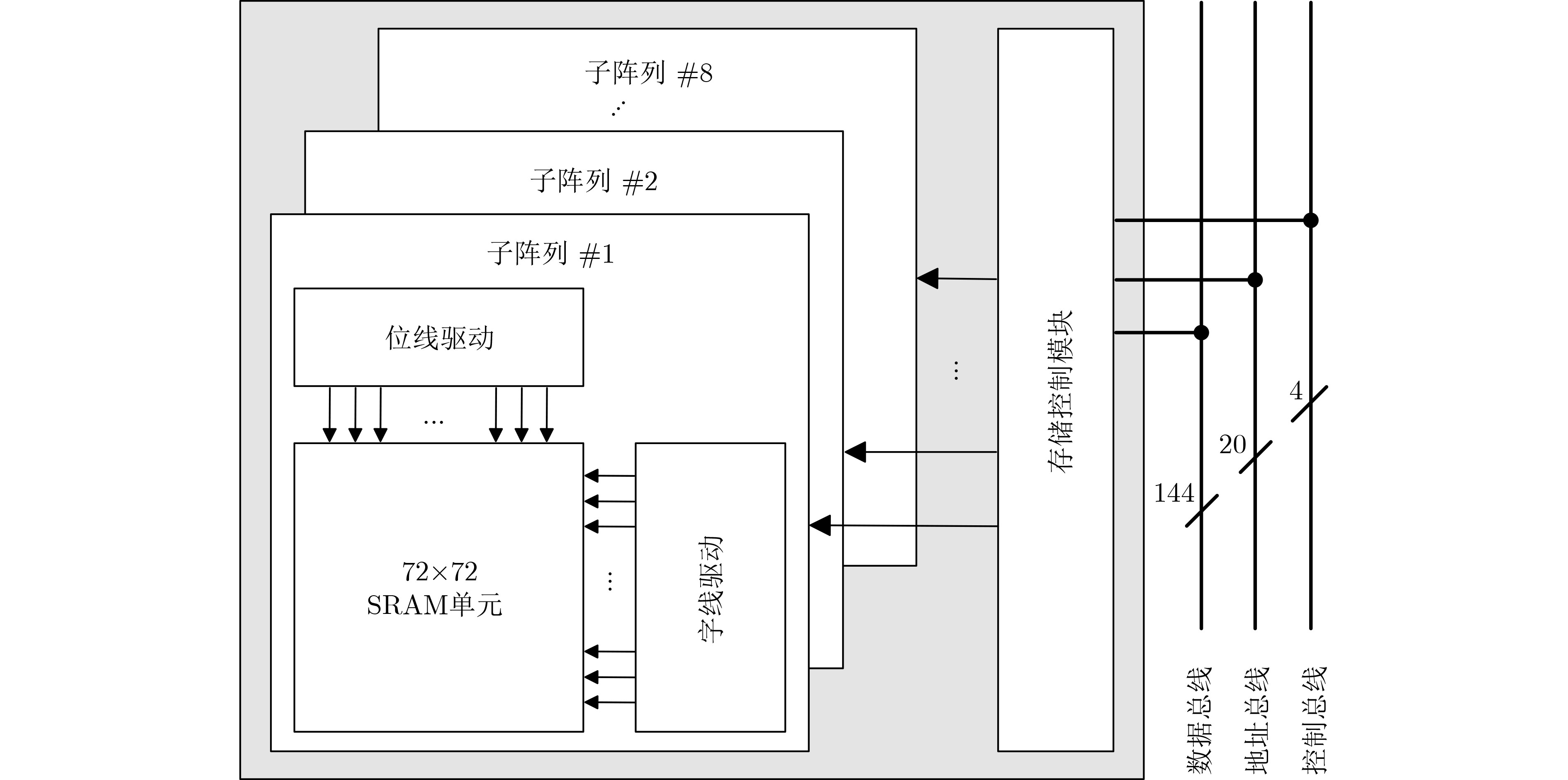
摘要: 视觉感知系统通过算法提取信息,但其能效受限于感知过程中数据转换与搬移的功耗开销。采用片上缓存实现边缘端系统中数据的存储与交互,通过减少对冗余信息的传输与搬运过程中的功耗,可有效降低系统的整体功耗。该研究提出了一种面向边缘计算的低功耗片上缓冲存储器(Cache)设计方案。该方案基于静态随机存取存储器(SRAM)单元,根据系统中二值神经网络层间数据量峰值,将缓存容量定制为40.5 kbit,集成在芯片内,专用于存储视觉感知系统的神经网络层间数据。针对传统单体式片上缓存功耗过高的问题,该方案采用分块式存储架构,依据二值神经网络最大池化层输出特征,将缓存阵列划分为8个独立可关断的72×72位子阵列。通过分块存储机制,数据存取过程中的动态功耗得到了有效降低。同时,该文进一步提出动态存储控制策略,利用卷积运算时层间数据量逐层递减的特性,在存取第2层卷积数据时,仅激活必要子阵列,由存储控制模块动态关闭未使用区块,实现功耗深度优化。在TSMC 180 nm CMOS工艺下仿真,结果表明时钟频率在10 MHz时,相较于单一式架构,分块式缓存在存储第1层卷积数据时,读写动态功耗降低64.97%;结合动态存储控制策略后,存储第2层卷积数据时的读写动态功耗进一步降低52.9%。该设计为边缘端视觉感知系统提供了高能效的片上存储解决方案。Abstract:
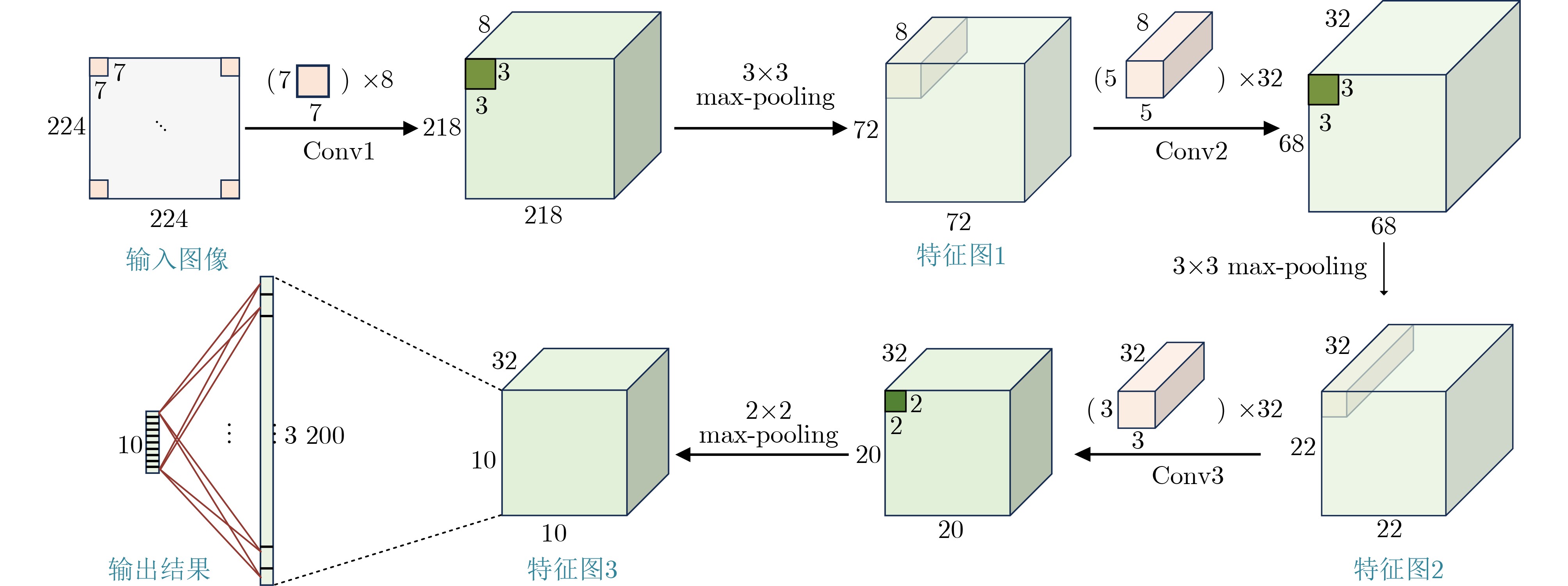
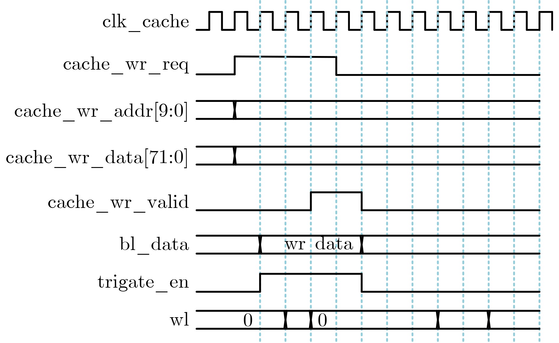
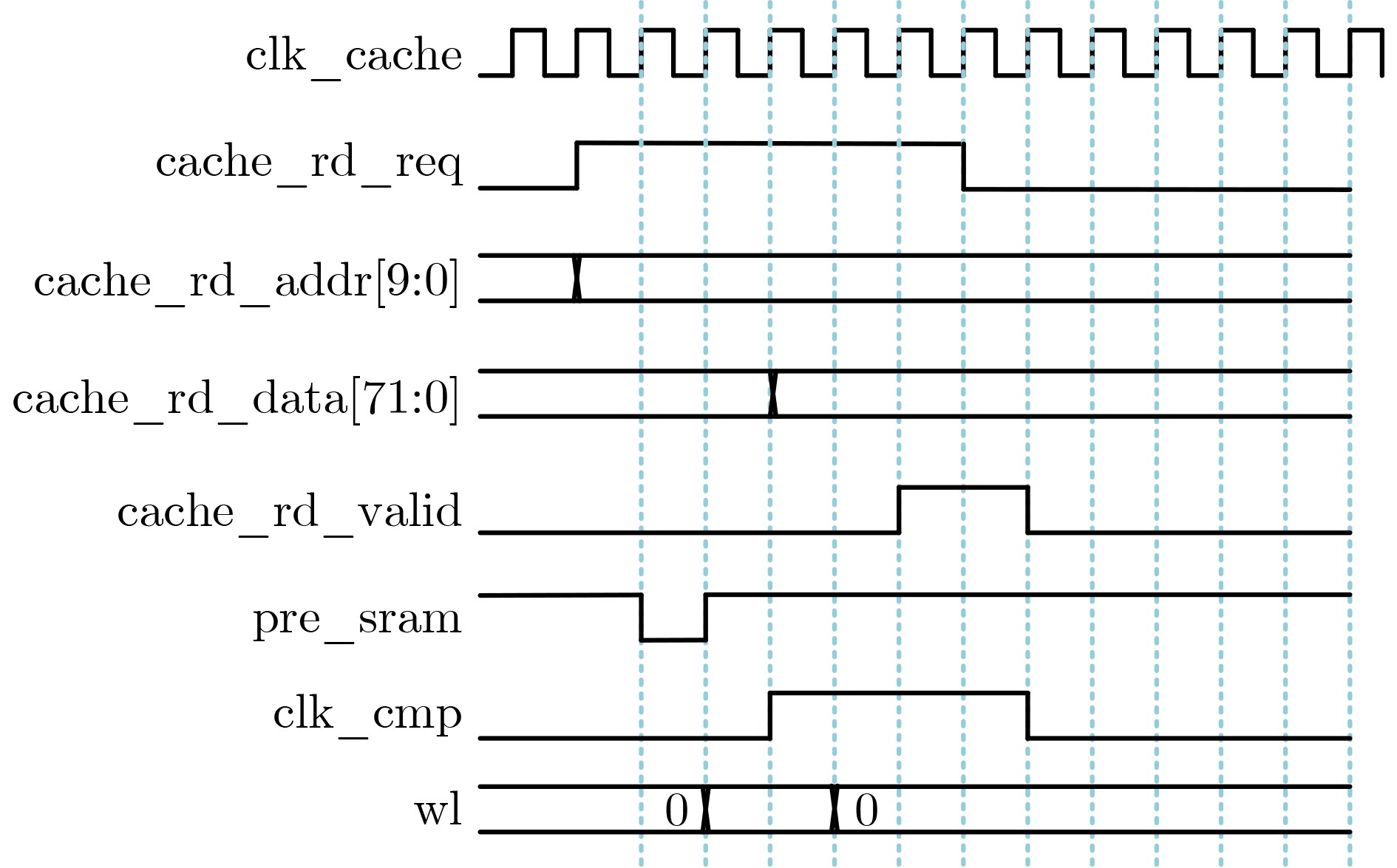
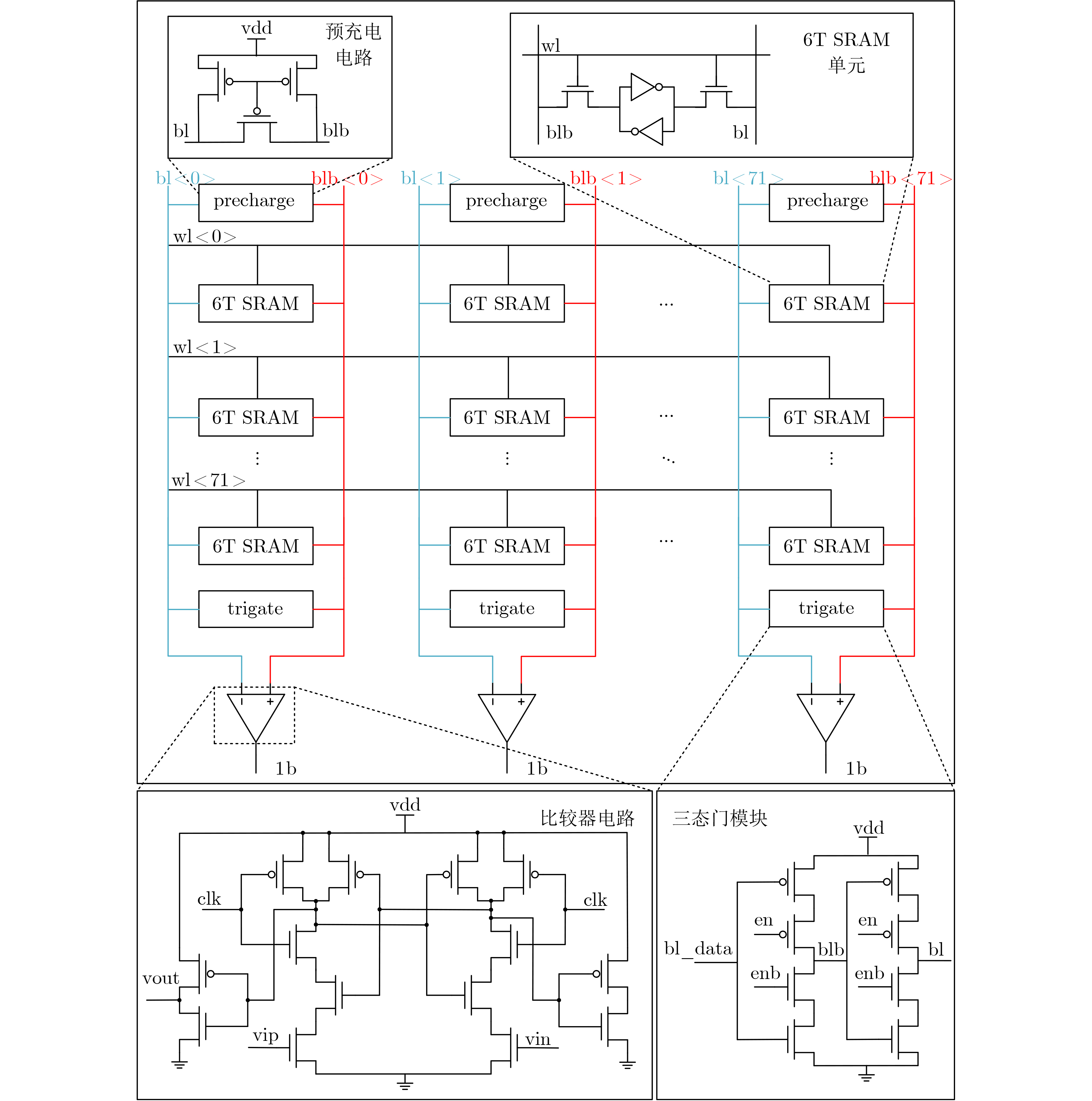
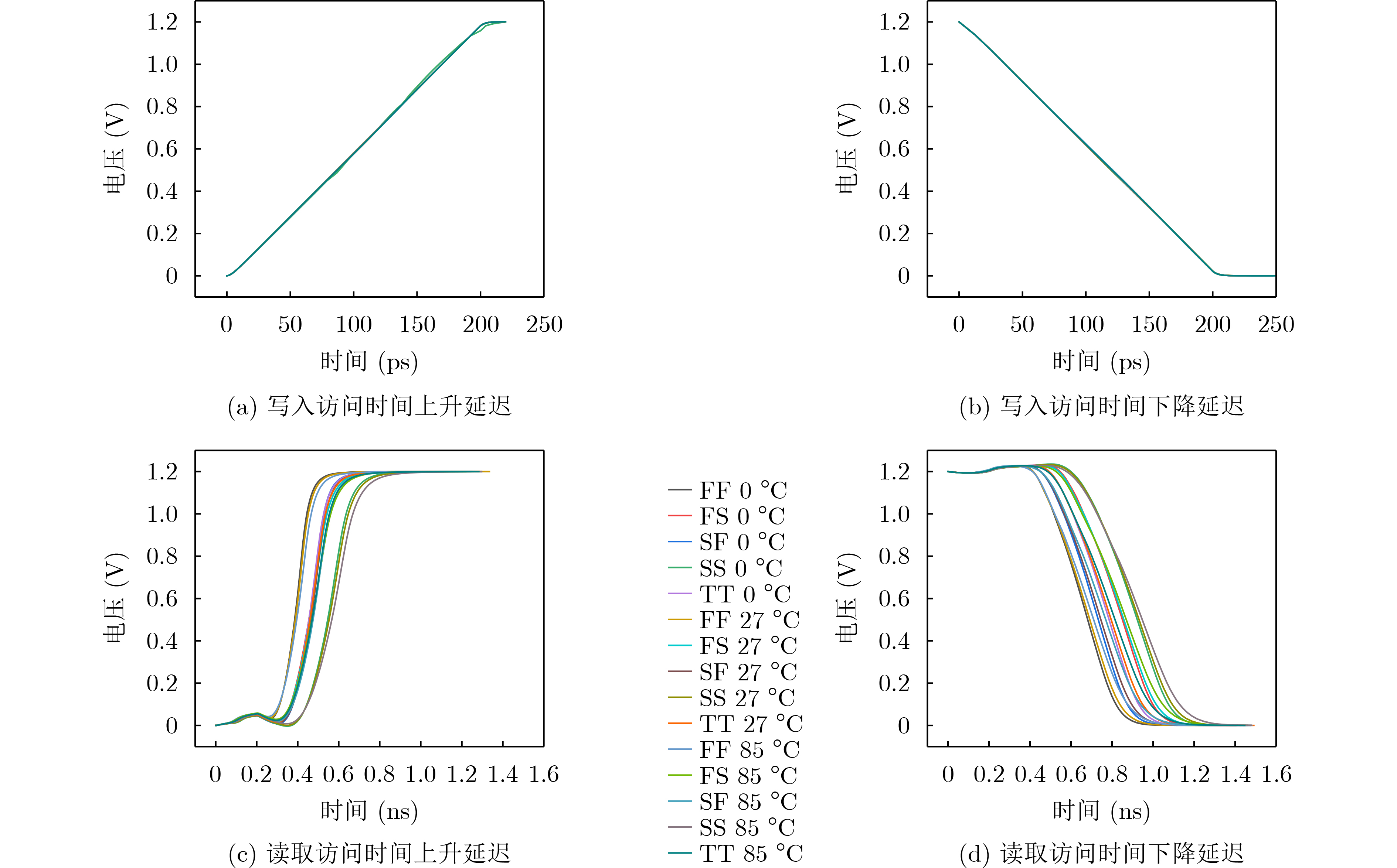
Objective The proliferation of Internet of Things (IoT) devices and the growing demand for edge computing have driven increased reliance on edge systems. However, deploying compute-intensive tasks on resource-constrained edge devices significantly raises computational demands and power consumption, thereby placing additional strain on energy-limited terminals. On-chip cache, which temporarily stores frequently accessed data and instructions, plays a crucial role in reducing latency and improving system performance. To address the stringent requirements of edge environments, it is essential to design on-chip caches that offer low power consumption, low manufacturing cost, and stable performance. Methods The proposed on-chip cache employs SRAM-based storage cells and a block-based architecture to store intermediate data between neural network layers. The memory capacity is configured as 40.5 kbit, based on the output feature map of the first neural network layer, which generates the largest data volume. This feature map has spatial dimensions of 72×72 with 8 channels. To enable efficient data scheduling during neural network computation, data from each channel is stored in an independent sub-array. Therefore, the buffer consists of 8 sub-arrays, each implemented as a 72×72 SRAM array with dedicated bit-line and word-line drivers. A memory control module is implemented to exploit the progressive reduction in data volume across convolutional layers. During access to the second convolutional layer, only the required sub-arrays are activated. Unused memory blocks are dynamically powered down by the control module to achieve deep power optimization. Performance evaluation is carried out through simulations using TSMC 180 nm CMOS technology. The evaluation includes measurements of access latency under different process corners and temperatures; read/write dynamic power consumption under varying supply voltages, temperatures, and clock frequencies; and a comparative analysis of dynamic power consumption between monolithic and block-based storage architectures. Results and Discussions The proposed on-chip cache demonstrates strong performance across key evaluation metrics. First, a comprehensive design summary is provided, detailing supply voltage, memory capacity, and layout area under different process variations ( Table 1 ). Second, dynamic read/write power measurements under varying operating temperatures, supply voltages, and clock frequencies (Tables 2 ~4 ) confirm excellent energy efficiency, satisfying the stringent power-performance requirements of edge visual sensing applications across diverse conditions. Access latency analysis further confirms stable memory read/write behavior under process corner variations and thermal fluctuations (Fig. 8 ). A comparative evaluation of power consumption between monolithic and partitioned storage architectures (Table 5 ), together with benchmarking against state-of-the-art designs (Table 6 ), demonstrates that the proposed cache achieves significantly lower read/write energy consumption at the same process node, while maintaining stable access characteristics at reduced operating voltages. This design adopts a system-level optimization strategy that emphasizes architectural innovation over costly process scaling. When implemented in more advanced technology nodes, the architecture is expected to achieve substantial gains in energy-per-access, minimum operating voltage, and area efficiency.Conclusions This paper presents the architecture and circuit-level design of an on-chip cache tailored for edge visual perception systems. By optimizing the cache structure for neural network workloads, the proposed design reduces dynamic power consumption through block-based storage and dynamic memory control, thereby enhancing energy efficiency and extending operational endurance. The approach offers broad applicability for edge-based visual perception devices. -
Key words:
- On-chip cache /
- Low power design /
- SRAM
-
表 1 设计总结
工艺 180 nm, 1P6M CMOS 电源电压 1.2 V 存储容量 40.5 kbit 72 bit × 72 bit × 8 bank 单元类型 SRAM 6T 单元版图大小 4.20 μm × 3.98 μm 存储器版图大小 1.2 mm × 0.8 mm 读写能耗 190.1 fJ/bit  下载: 导出CSV
表 2 不同时钟频率下读写操作动态功耗
时钟频率(MHz) 温度( °C) 电源电压(V) 写操作动态功耗(μW) 读操作动态功耗(μW) 总动态功耗(μW) 10 27 1.2 14.24 15.04 29.28 20 35.75 34.65 70.40 40 70.14 68.06 138.20
下载: 导出CSV
表 3 不同温度下读写操作动态功耗
温度( °C) 时钟频率(MHz) 电源电压(V) 写操作动态功耗(μW) 读操作动态功耗(μW) 总动态功耗(μW) 0 10 1.2 17.50 17.11 34.61 27 14.24 15.04 29.28 85 30.03 29.23 59.26
下载: 导出CSV
表 4 不同电源电压下读写操作动态功耗
电源电压(V) 温度( °C) 时钟频率(MHz) 写操作动态功耗(μW) 读操作动态功耗(μW) 总动态功耗(μW) 0.8 27 10 6.82 8.08 14.90 1.0 11.87 12.54 24.41 1.2 14.24 15.04 29.28
下载: 导出CSV
表 5 单一式与分块存储式片上缓冲存储器存储不同卷积层数据时的读写动态功耗
片上缓存策略 温度( °C) 时钟频率(MHz) 电源电压(V) 卷积层 写操作动态功耗(μW) 读操作动态功耗(μW) 总动态功耗(μW) 单一式 27 10 1.2 Conv1 34.78 48.80 83.58 分块存储 27 10 1.2 Conv1 14.24 15.04 29.28 Conv2 6.97 6.82 13.79
下载: 导出CSV
-
[1] YANG Zhen, ZHANG Jie, JIANG Yunliang, et al. A self-organizing IoT service perception algorithm based on human visual direction-sensitive system[J]. IEEE Internet of Things Journal, 2023, 10(7): 6193–6204. doi: 10.1109/JIOT.2022.3223039. [2] RASTOGI A, KUMAR S, AGGARWAL A, et al. IoT-based smart traffic monitoring and control system for urban areas[C]. 2025 Fourth International Conference on Smart Technologies, Communication and Robotics, Sathyamangalam, India, 2025: 1–6. doi: 10.1109/STCR62650.2025.11018946. [3] CHEN Jiao, HE Jiayi, CHEN Fangfang, et al. Empowering IoT-based autonomous driving via federated instruction tuning with feature diversity[J]. IEEE Internet of Things Journal, 2025, 12(6): 6095–6108. doi: 10.1109/JIOT.2024.3518615. [4] RIZZO L, ZICARI P, CICIRELLI F, et al. A study on consumer-grade EEG headsets in BCI applications[C]. 2024 IEEE Conference on Pervasive and Intelligent Computing, Boracay Island, Philippines, 2024: 67–74. doi: 10.1109/PICom64201.2024.00016. [5] YEOLE P, LABADE Y, WABALE N, et al. IoT-enabled smart wearables for improved visual impairment navigation[C]. 2024 International Conference on Decision Aid Sciences and Applications, Manama, Bahrain, 2024: 1–5. doi: 10.1109/DASA63652.2024.10836578. [6] ABBAS N, ZHANG Yan, TAHERKORDI A, et al. Mobile edge computing: A survey[J]. IEEE Internet of Things Journal, 2018, 5(1): 450–465. doi: 10.1109/JIOT.2017.2750180. [7] WANG Sai, LI Xiaoyang, and GONG Yi. Energy-efficient task offloading and resource allocation for delay-constrained edge-cloud computing networks[J]. IEEE Transactions on Green Communications and Networking, 2024, 8(1): 514–524. doi: 10.1109/TGCN.2023.3306002. [8] LI Ziwei, XU Han, LIU Zheyu, et al. A 2.17μW@120fps ultra-low-power dual-mode CMOS image sensor with senputing architecture[C]. 2022 27th Asia and South Pacific Design Automation Conference, Taipei, China, 2022: 92–93. doi: 10.1109/ASP-DAC52403.2022.9712591. [9] PUVIRAJAN T, PAULRAJ R L, KULKARNI S, et al. 6T SRAM: A technical overview[C]. 2023 International Conference on Advances in Electronics, Communication, Computing and Intelligent Information Systems, Bangalore, India, 2023: 698–702. doi: 10.1109/ICAECIS58353.2023.10170407. [10] SINGH T, PRAKASH V, ANWER S S, et al. Analyzing the performance of 6T SRAM cell and 64×64 memory array at lower technology nodes for low power design[C]. 2023 1st International Conference on Circuits, Power and Intelligent Systems, Bhubaneswar, India, 2023: 1–6. doi: 10.1109/CCPIS59145.2023.10291492. [11] YU Shimeng, JIANG Hongwu, HUANG Shanshi, et al. Compute-in-memory chips for deep learning: Recent trends and prospects[J]. IEEE Circuits and Systems Magazine, 2021, 21(3): 31–56. doi: 10.1109/MCAS.2021.3092533. [12] MITTAL S and VETTER J S. A survey of software techniques for using non-volatile memories for storage and main memory systems[J]. IEEE Transactions on Parallel and Distributed Systems, 2016, 27(5): 1537–1550. doi: 10.1109/TPDS.2015.2442980. [13] INCI A, ISGENC M M, and MARCULESCU D. DeepNVM++: Cross-layer modeling and optimization framework of nonvolatile memories for deep learning[J]. IEEE Transactions on Computer-Aided Design of Integrated Circuits and Systems, 2022, 41(10): 3426–3437. doi: 10.1109/TCAD.2021.3127148. [14] RATHI N, KUMAR A, GUPTA N, et al. A review of low-power static random access memory (SRAM) designs[C]. 2023 IEEE Devices for Integrated Circuit, Kalyani, India, 2023: 455–459. doi: 10.1109/DevIC57758.2023.10134887. [15] SIMON W A, LEVISSE A, ZAPATER M, et al. A hybrid cache HW/SW stack for optimizing neural network runtime, power and endurance[C]. 2020 IFIP/IEEE 28th International Conference on Very Large Scale Integration, Salt Lake City, USA, 2020: 94–99. doi: 10.1109/VLSI-SOC46417.2020.9344087. [16] NAZEMIAN M and SAYEDI S M. Low power SRAM using an optimal number of split bit lines and single-ended sensing[C]. 2023 31st International Conference on Electrical Engineering, Tehran, Islamic Republic of Iran, 2023: 947–950. doi: 10.1109/ICEE59167.2023.10334788. [17] NGUYEN D T, BHATTACHARJEE A, MOITRA A, et al. MCAIMem: A mixed SRAM and eDRAM cell for area and energy-efficient on-chip AI memory[J]. IEEE Transactions on Very Large Scale Integration (VLSI) Systems, 2024, 32(11): 2023–2036. doi: 10.1109/TVLSI.2024.3439231. [18] NAZHAMAITI M, JIANG Weihuang, SU Haijin, et al. Selfputing: A 0.57 μW @ 15 fps vision chip with self-powered in-pixel computing and in-memory computing for visual perception on the edge[C]. 2024 IEEE European Solid-State Electronics Research Conference, Bruges, Belgium, 2024: 585–588. doi: 10.1109/ESSERC62670.2024.10719556. [19] COSEMANS S, DEHAENE W, and CATTHOOR F. A low-power embedded SRAM for wireless applications[J]. IEEE Journal of Solid-State Circuits, 2007, 42(7): 1607–1617. doi: 10.1109/JSSC.2007.896693. [20] COSEMANS S, DEHAENE W, and CATTHOOR F. A 3.6pJ/access 480MHz, 128Kbit on-Chip SRAM with 850MHz boost mode in 90nm CMOS with tunable sense amplifiers to cope with variability[C]. 34th European Solid-State Circuits Conference, Edinburgh, UK, 2008: 278–281. doi: 10.1109/ESSCIRC.2008.4681846. [21] CHEN Yuzong, MU Junjie, KIM H, et al. BP-SCIM: A reconfigurable 8T SRAM macro for bit-parallel searching and computing in-memory[J]. IEEE Transactions on Circuits and Systems I: Regular Papers, 2023, 70(5): 2016–2027. doi: 10.1109/TCSI.2023.3240303. -


图(8) / 表(6)
计量
- 文章访问数: 461
- HTML全文浏览量: 268
- PDF下载量: 43
- 被引次数: 0
 下载:
下载:
