Advanced Search
Turn off MathJax
Article Contents
LI Pan, DUAN Chuangwei, ZHU Wenbo, YANG Lixia, LIAO Guisheng. Design of a Low-Cost High-Isolation RF Switch for X-Band Active Phased Array T/R Modules[J]. Journal of Electronics & Information Technology. doi: 10.11999/JEIT260326
Citation: LI Pan, DUAN Chuangwei, ZHU Wenbo, YANG Lixia, LIAO Guisheng. Design of a Low-Cost High-Isolation RF Switch for X-Band Active Phased Array T/R Modules[J]. Journal of Electronics & Information Technology. doi: 10.11999/JEIT260326

Design of a Low-Cost High-Isolation RF Switch for X-Band Active Phased Array T/R Modules

doi: 10.11999/JEIT260326 cstr: 32379.14.JEIT260326
Funds:  National Natural Science Foundation of China (62501001), Supported by the Project of the National Key R&D Program of China (2024YFB3908202), Anhui Provincial Natural Science Foundation (2508085QF236), General Program of the China Postdoctoral Science Foundation (2025M780492), Anhui Postdoctoral Scientific Research Program Foundation (2026A1274)
  • Received Date: 2026-03-26
  • Accepted Date: 2026-09-15
  • Rev Recd Date: 2026-09-15
  • Available Online: 2026-09-20
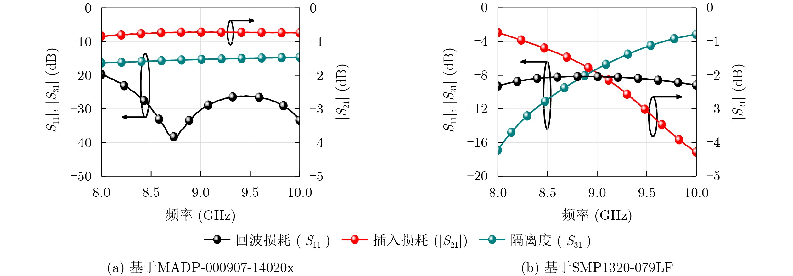
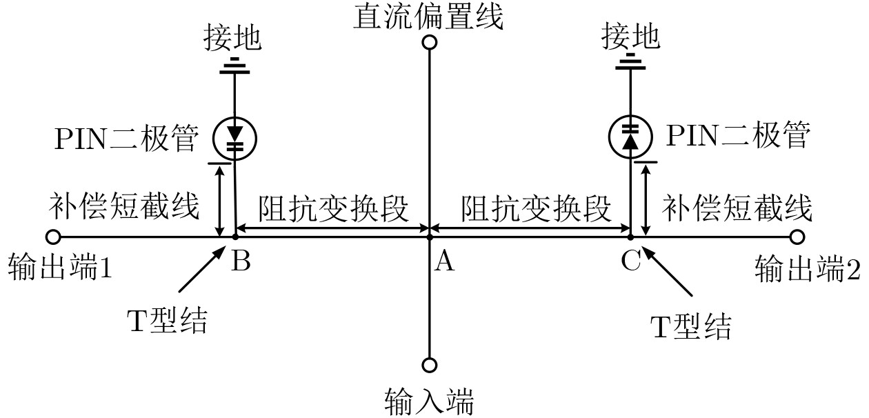
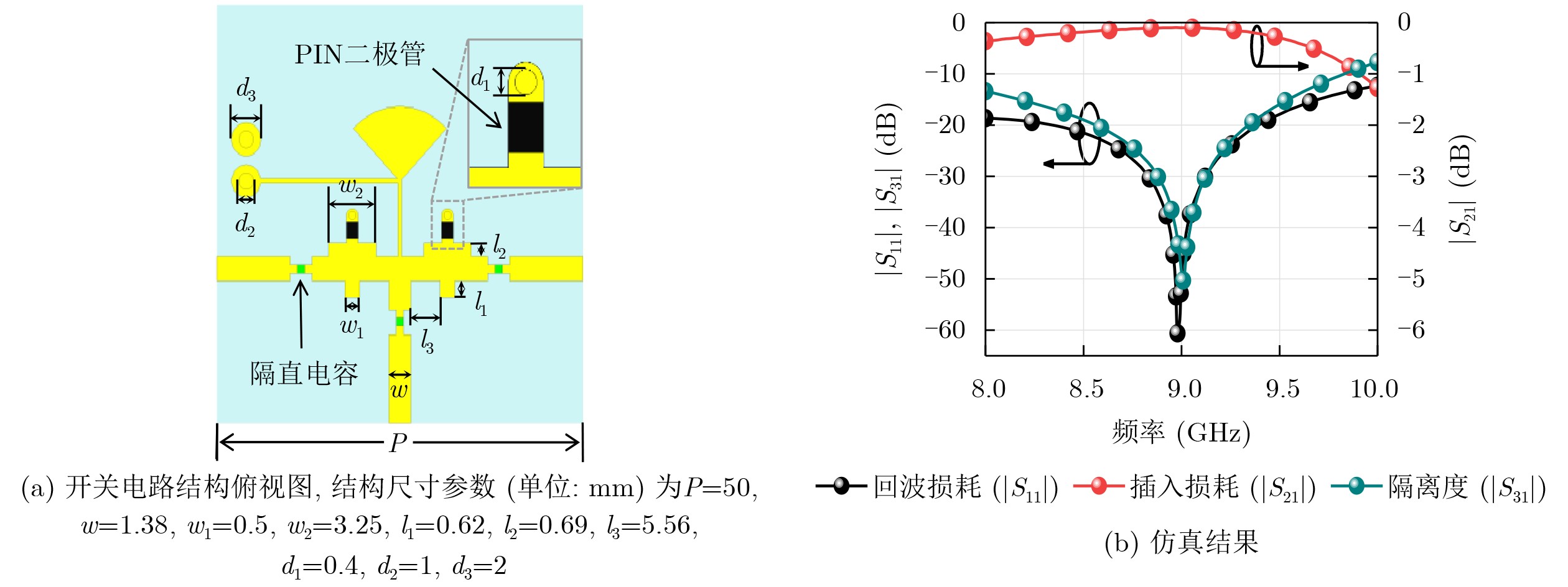
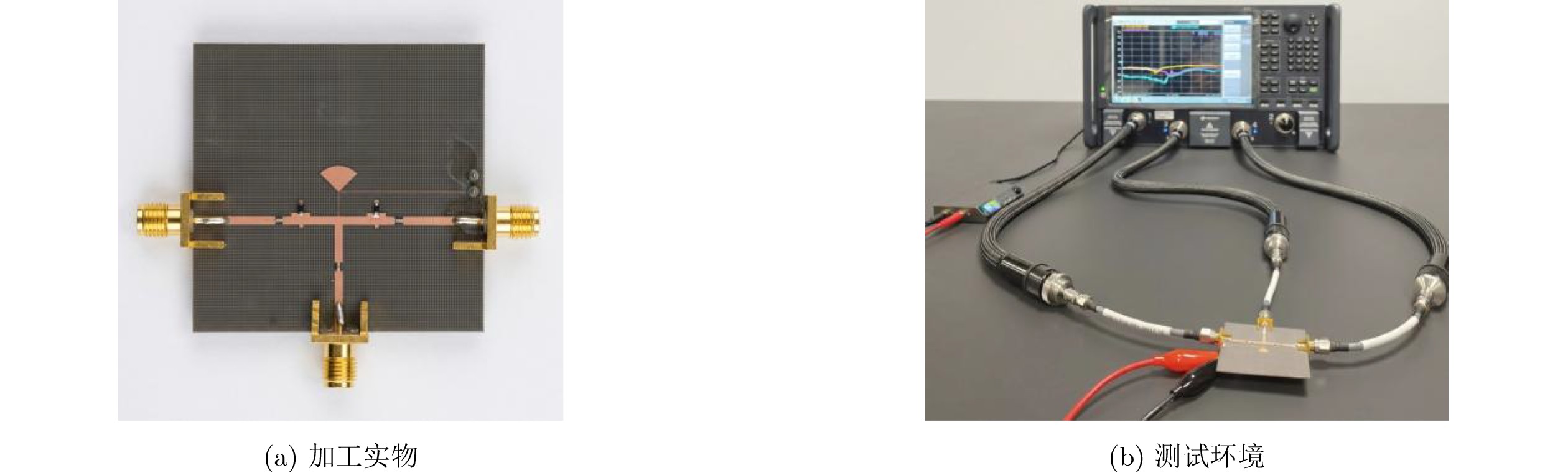
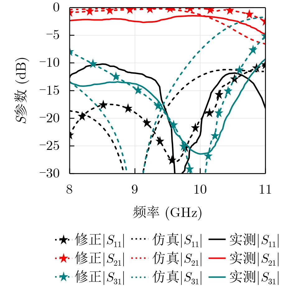
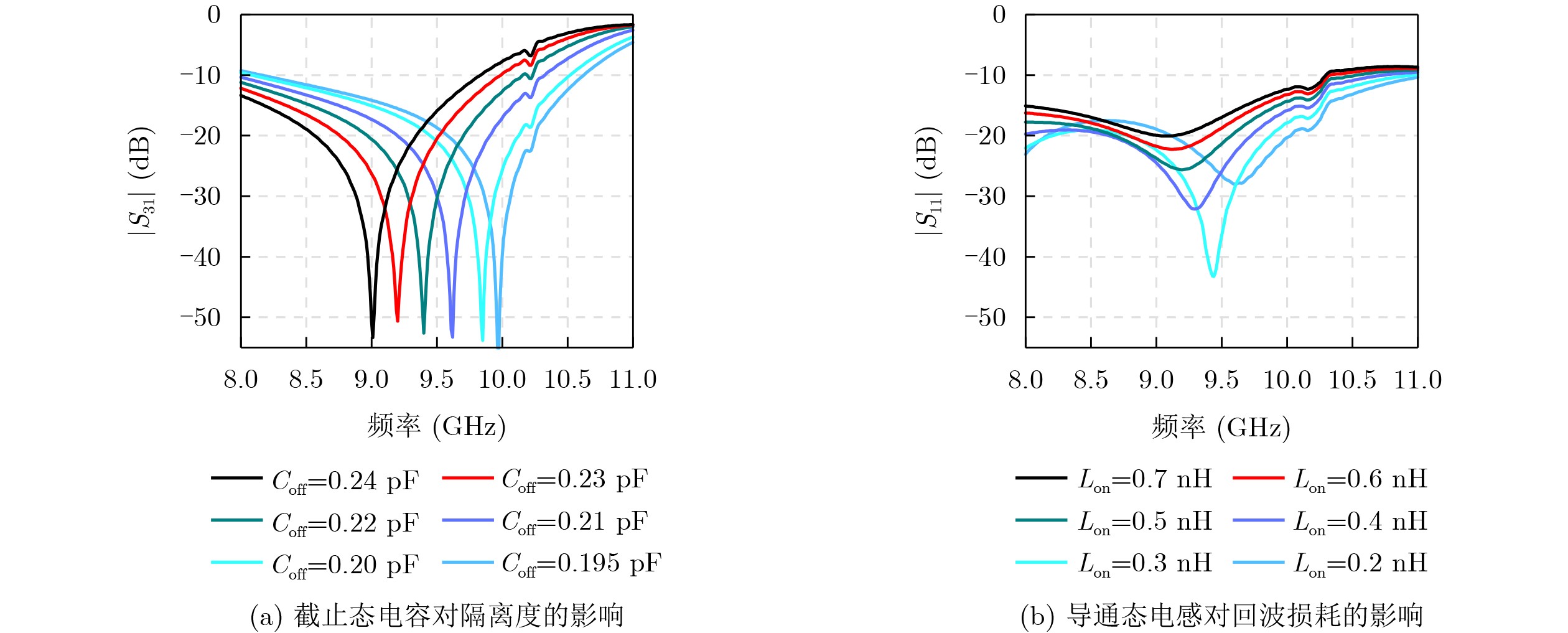
  •   Objective  Radio frequency (RF) switches are key front-end components in communication and radar systems, especially in active phased array transmit/receive (T/R) modules. Positive-intrinsic-negative (PIN) diodes are widely used in high-power microwave switches because of their high power-handling capability, good linearity, and mature fabrication process. However, low-cost plastic-packaged PIN diodes exhibit significant parasitic effects at X-band frequencies. Junction capacitance, package inductance, and grounding-via inductance cause shunt branches to deviate from ideal short- or open-circuit conditions, resulting in degraded isolation and increased insertion loss. To address this problem, a low-cost high-isolation X-band single-pole double-throw (SPDT) RF switch design method based on parasitic-parameter compensation is proposed.  Methods  A step-wise synergistic matching strategy, termed “OFF-state prioritized determination and ON-state structural compensation”, is developed. OFF-state isolation and ON-state transmission conditions are treated separately to reduce coupling between isolation and transmission objectives. For the isolation branch, OFF-state diode parasitic parameters, a compensation stub, and grounding-via inductance are combined to form a series-resonant network. By compensating parasitic reactance, the branch satisfies the required impedance condition and suppresses signal leakage. After the compensation-stub parameters are determined, ON-state compensation is realized by introducing equivalent structural capacitance through T-junction edge effects and a stepped-impedance main line. This capacitance, together with the total equivalent inductance of the shunt branch, forms a parallel-resonant network, making the branch approach an open-circuit condition at the operating frequency. Thus, signal shunting is reduced and low-insertion-loss transmission is achieved without additional lumped compensation components.  Results and Discussions  The proposed switch topology is presented, and a full-wave simulation model is established (Fig. 3, Fig. 4(a)). Simulation results show that return loss is better than 20 dB, isolation is higher than 20 dB, and insertion loss remains around 0.2 dB over 8.57–9.34 GHz (Fig. 4(b)). A prototype is fabricated and measured (Fig. 5). Measurement results show that, over 9.5–10.4 GHz, return loss is better than 10 dB, insertion loss is lower than 2 dB, and isolation is higher than 20 dB (Fig. 6). Although the measured operating band shifts upward by about 1 GHz relative to initial simulation results, measured trends remain consistent with theoretical analysis. To explain this frequency shift, OFF-state junction capacitance and ON-state parasitic inductance are further analyzed. As OFF-state junction capacitance decreases from 0.24 pF to 0.195 pF, the high-isolation band shifts to higher frequencies (Fig. 7(a)). With OFF-state capacitance fixed at 0.195 pF, reducing ON-state parasitic inductance from 0.7 nH to 0.2 nH shifts the return-loss response to higher frequencies (Fig. 7(b)). After parameter correction, simulated return loss, insertion loss, and isolation agree more closely with measured results (Fig. 6). Compared with existing SPDT RF switch designs, the proposed design uses low-cost plastic-packaged PIN diodes and a simple microstrip compensation structure, requires no additional lumped compensation components, reduces dependence on the high intrinsic OFF-state impedance of PIN diodes, and achieves a good balance between cost and high-frequency switch performance (Table 1).  Conclusions  A low-cost high-isolation X-band SPDT RF switch based on parasitic-parameter compensation is presented. By using OFF-state series resonance and ON-state structural capacitance compensation, high isolation and low insertion loss are realized simultaneously. The fabricated switch achieves isolation higher than 20 dB and insertion loss lower than 2 dB over 9.5-10.4 GHz. The switch features a simple structure, ease of integration, and low cost, and provides a practical reference for low-cost high-isolation T/R module RF switches in active phased array systems.
  • loading
  • [1]
    HAIDER J, KHAN W, NADEEM A, et al. Design of a compact T/R module for an all-digital S-band phased array radar system[C]. 2025 2nd International Conference on Microwave, Antennas & Circuits (ICMAC), Islamabad, Pakistan, 2025: 1–4. doi: 10.1109/ICMAC64768.2025.11003263.
    [2]
    SHAO Bingqian, LU Chengjian, XIANG Yinjie, et al. Comprehensive review of RF MEMS switches in satellite communications[J]. Sensors, 2024, 24(10): 3135. doi: 10.3390/s24103135.
    [3]
    YOU Changsheng, CAI Yunlong, LIU Yuanwei, et al. Next generation advanced transceiver technologies for 6G and beyond[J]. IEEE Journal on Selected Areas in Communications, 2025, 43(3): 582–627. doi: 10.1109/JSAC.2025.3536557.
    [4]
    REBEIZ G M and MULDAVIN J B. RF MEMS switches and switch circuits[J]. IEEE Microwave Magazine, 2001, 2(4): 59–71. doi: 10.1109/6668.969936.
    [5]
    KURMENDRA and AGARWAL S. MEMS switch realities: Addressing challenges and pioneering solutions[J]. Micromachines, 2024, 15(5): 556. doi: 10.3390/mi15050556.
    [6]
    TAIT R N. Progress in RF-MEMS[J]. Micromachines, 2025, 16(2): 233. doi: 10.3390/mi16020233.
    [7]
    LI Qiqi, LENG Yongqing, QIU Xin, et al. A 6–18 GHz high power-handling switch in GaN technology[C]. 2023 IEEE MTT-S International Microwave Workshop Series on Advanced Materials and Processes for RF and THz Applications (IMWS-AMP), Chengdu, China, 2023: 1–3. doi: 10.1109/IMWS-AMP57814.2023.10381466.
    [8]
    HUANG C T, LIN Y S, HUANG C Y, et al. Design and analysis of SPDT switch and array antenna for 28 GHz 5G new radio[C]. 2024 IEEE/MTT-S International Microwave Symposium - IMS 2024, Washington, USA, 2024: 757–759. doi: 10.1109/IMS40175.2024.10600305.
    [9]
    TSAO C M and HSU H T. An ultra-wideband, high power and high isolation single-pole-double-throw switch using capacitive loading approach[J]. IEEE Transactions on Circuits and Systems II: Express Briefs, 2023, 70(11): 4013–4017. doi: 10.1109/TCSII.2023.3286884.
    [10]
    ZHOU Pinhao, SHEN Guangxu, FENG Wenjie, et al. A compact wideband SPDT switch using compensating inductors and highpass matching network[J]. IEEE Transactions on Circuits and Systems I: Regular Papers, 2025, 72(8): 3961–3970. doi: 10.1109/TCSI.2024.3479424.
    [11]
    HSIEH Y C, LIN G J, TSAI Z M, et al. A Q-/V-band 37.6-dBm IP0.1 dB and low loss SPDT switch using three-series PIN diodes connection[J]. International Journal of Microwave and Wireless Technologies, 2025, 17(4): 731–739. doi: 10.1017/S175907872510175X.
    [12]
    PARK J, LEE S, and HONG S. A 24–40 GHz differential SPDT switch with an NMOS and PMOS alternating structure and leakage-canceling capacitors[J]. IEEE Transactions on Circuits and Systems II: Express Briefs, 2023, 70(1): 86–90. doi: 10.1109/TCSII.2022.3205907.
    [13]
    FORBES T, SAUGEN J, and MAGSTADT B. Differential cancellation based RF switch enabling high isolation and minimal insertion loss in 0.0006 mm2 area[C]. 2022 IEEE Texas Symposium on Wireless and Microwave Circuits and Systems (WMCS), Waco, USA, 2022: 1–4. doi: 10.1109/WMCS55582.2022.9866179.
    [14]
    GHORBANI F, ZHOU Jiafeng, HUANG Yi, et al. Impedance-oriented approach for maximizing linearity in p-i-n-diode-based phase shifters[J]. IEEE Transactions on Microwave Theory and Techniques, 2025, 73(8): 4513–4522. doi: 10.1109/TMTT.2025.3547970.
    [15]
    LIU Mingming, JIN Ronghong, GENG Junping, et al. Low-insertion loss PIN diode switches using impedance-transformation networks[J]. Progress in Electromagnetics Research C, 2013, 34: 195–202. doi: 10.2528/PIERC12092604.
    [16]
    VASSILEV V, VILENSKIY A, CHOU H T, et al. A 55-105 GHz PIN diode SPDT switch[C]. 2021 International Symposium on Antennas and Propagation (ISAP), Taipei, China, 2021: 1–2. doi: 10.23919/ISAP47258.2021.9614359.
    [17]
    SINGH A and MANDAL M K. Parasitic compensation and hence isolation improvement of PIN diode-based switches[J]. IEEE Transactions on Circuits and Systems II: Express Briefs, 2021, 68(1): 97–101. doi: 10.1109/TCSII.2020.3000587.
    [18]
    ZHANG Yi, ZHOU Yingjie, LU Xinmin, et al. X-band high isolation single pole double throw switch based on resonant concept[J]. Microwave and Optical Technology Letters, 2024, 66(6): e34221. doi: 10.1002/mop.34221.
    [19]
    MOON S, KWON J, LEE J, et al. X-band asymmetric GaN HEMT SPDT switch using LC resonator and quarter-wave stub for high power handling capability and high isolation[C]. 2025 20th European Microwave Integrated Circuits Conference (EuMIC), Utrecht, Netherlands, 2025: 339–342. doi: 10.23919/EuMIC65284.2025.11234504.
    [20]
    POZAR D M. Microwave Engineering[M]. 4th ed. Hoboken: John Wiley & Sons, 2011: 56–74, 272–277. (查阅网上资料, 未找到本条文献出版地信息, 请确认).
    [21]
    GUPTA K C, GARG R, BAHL I, et al. Microstrip Lines and Slotlines[M]. 2nd ed. Boston: Artech House, 1996: 189–208.
  • 加载中

Catalog

    通讯作者: 陈斌, bchen63@163.com
    • 1. 

      沈阳化工大学材料科学与工程学院 沈阳 110142

    1. 本站搜索
    2. 百度学术搜索
    3. 万方数据库搜索
    4. CNKI搜索

    Figures(7)  / Tables(1)

    Article Metrics

    Article views (16) PDF downloads(0) Cited by()
    Proportional views
    Related

    /

    DownLoad:  Full-Size Img  PowerPoint
    Return
    Return